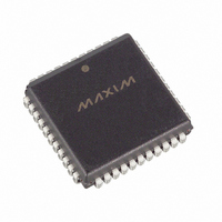
DS2141AQ+ Maxim Integrated Products, DS2141AQ+ Datasheet - Page 26

DS2141AQ+
Manufacturer Part Number
DS2141AQ+
Description
IC CONTROLLER T1 5V 44-PLCC
Manufacturer
Maxim Integrated Products
Datasheet
1.DS2141AQ.pdf
(39 pages)
Specifications of DS2141AQ+
Controller Type
T1 Controller
Interface
Parallel/Serial
Voltage - Supply
4.5 V ~ 5.5 V
Current - Supply
10mA
Operating Temperature
0°C ~ 70°C
Mounting Type
Surface Mount
Package / Case
44-LCC, 44-PLCC
Operating Supply Voltage
5 V
Supply Current (max)
10 mA
Maximum Operating Temperature
+ 70 C
Minimum Operating Temperature
0 C
Mounting Style
SMD/SMT
Lead Free Status / RoHS Status
Lead free / RoHS Compliant
frame boundaries (RCR2.3 = 0). If the user wishes to obtain pulses at the frame boundary, then RCR2.4
must be set to 0; if the user wishes to have pulses occur at the multiframe boundary, then RCR2.4 must be
set to 1. If the user selects to apply a 2.048 MHz clock to the SYSCLK pin, then the data output at RSER
will be forced to all 1's every fourth channel and the F-bit will be deleted. Hence channels 1, 5, 9, 13, 17,
21, 25, and 29 (timeslots 0, 4, 8, 12, 16, 20, 24, and 28) will be forced to a 1. Also, in 2.048 MHz
applications, the RCHBLK output will be forced high during the same channels as the RSER pin. See
Section 13 for more details. This is useful in T1 to CEPT (E1) conversion applications. If the 386-bit
elastic buffer either fills or empties, a controlled slip will occur. If the buffer empties, then a full frame of
data (193 bits) will be repeated at RSER and the SR1.4 and RIR.3 bits will be set to a 1. If the buffer fills,
then a full frame of data will be deleted and the SR1.4 and RIR.4 bits will be set to a 1.
10.2 Transmit Side
The transmit side elastic store can only be used if the receive side elastic store is enabled. The operation
of the transmit elastic store is very similar to the receive side; both have controlled slip operation and both
can operate with either a 1.544 MHz or a 2.048 MHz SYSCLK. When the transmit elastic store is
enabled, both the SYSCLK and RSYNC signals are shared by both the elastic stores. Hence, they will
have the same backplane PCM frame and data structure. Controlled slips in the transmit elastic store are
reported in by setting both RIR.3 and RIR.4.
11.0 RECEIVE MARK REGISTERS
The DS2141A has the ability to replace the incoming data, on a channel-by-channel basis, with either an
idle code (7F Hex) or the digital milliwatt code, which is an 8-byte repeating pattern that represents a 1
kHz sine wave (1E/0B/0B/1E/9E/8B/8B/9E). The RCR2.7-bit will determine which code is used. Each
bit in the RMRs represents a particular channel. If a bit is set to a 1, then the receive data in that channel
will be replaced with one of the two codes. If a bit is set to 0, no replacement occurs.
RMR1/RMR2/RMR3: RECEIVE MARK REGISTERS (2Dh to 2Fh)
(MSB)
12.0 LINE INTERFACE CONTROL FUNCTION
The DS2141A can control line interface units that contain serial ports. When Control Register Bytes 1 or
2 (CRB1, CRB2) are written to, the DS2141A will automatically write this data serially (LSB first) into
the line interface by creating a chip select, serial clock and serial data via the
LI_SDI pins respectively. This control function is driven off of the RCLK; therefore RCLK must be
present for proper operation. Registers CRB1 and CRB2 can only be written to, not read from. Writes to
these registers must be at least 20 sec apart. See Section 13 for timing information.
CH16
CH24
CH8
SYMBOL
CH24
CH1
CH15
CH23
CH7
POSITION
RMR3.7
RMR1.0
CH14
CH22
CH6
CH13
CH21
CH5
NAME AND DESCRIPTION
Receive Mark Registers.
0=do not affect the receive data associated with this channel.
1=replace the receive data associated with this channel with either
the idle code or the digital milliwatt code.
CH12
CH20
CH4
26 of 39
CH11
CH19
CH3
CH10
CH18
CH2
CH17
CH1
CH9
(LSB)
LI_CS
, LI_SCLK and
RMR1 (2D)
RMR2 (2E)
RMR3 (2F)
DS2141A


