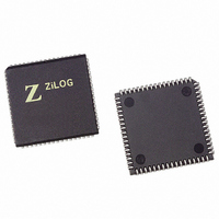
Z16C3516VSG Zilog, Z16C3516VSG Datasheet - Page 111

Z16C3516VSG
Manufacturer Part Number
Z16C3516VSG
Description
IC 16MHZ Z8500 CMOS ISCC 68-PLCC
Manufacturer
Zilog
Series
IUSC™r
Specifications of Z16C3516VSG
Controller Type
Serial Communications Controller (SCC)
Interface
USB
Voltage - Supply
4.75 V ~ 5.25 V
Current - Supply
50mA
Operating Temperature
0°C ~ 70°C
Mounting Type
Surface Mount
Package / Case
68-LCC (J-Lead)
Lead Free Status / RoHS Status
Lead free / RoHS Compliant
Other names
269-4690-5
Z16C3516VSG
Z16C3516VSG
Available stocks
Company
Part Number
Manufacturer
Quantity
Price
Company:
Part Number:
Z16C3516VSG
Manufacturer:
INTEL
Quantity:
6 219
- Current page: 111 of 268
- Download datasheet (3Mb)
UM011001-0601
INTERRUPT ACKNOWLEDGE CYCLES
The primary timing differences between the Z80 CPUs and
Z8500 peripherals occur in the Interrupt Acknowledge
cycle. The Z8500 timing parameters that are significant
during Interrupt Acknowledge cycles are listed in Table 16,
while the Z80 parameters are listed in Table 17. The
reference numbers in Tables 16 and 17 refer to Figures 10,
12 and 13.
If the CPU and the peripherals are running at different
speeds (as with the Z80H interface), the /INTACK signal
must
Synchronization is discussed in detail under Interrupt
Acknowledge for Z80H CPU to Z8500/8500A Peripherals.
During an Interrupt Acknowledge cycle, Z8500 peripherals
require both /INTACK and /RD to be active at certain
EXTERNAL INTERFACE LOGIC
The following sections discuss external interface logic
required during Interrupt Acknowledge cycles for each
interface type.
CPU/Peripheral Same Speed
Figure 9 shows the logic used to interface the Z80A CPU
to the Z8500 peripherals and the Z80B CPU to Z8500A
Worst Case
1.
2.
5.
3.
.
Worst Case
TdC(M1f)
TdM1f(IORQf)
4. TsD(Cr)
TsIA(PC)
ThIA(PC)
TdIAi(RD)
TwRDA
TdRDA(DR)
TsIEI(RDA)
ThIEI(RDA)
TdIEI(IE)
be
synchronized
Table 16. Z80 CPU Timing Parameters Interrupt Acknowledge Cycles
Clock High to /M1 Low Delay
/M1 Low to /IORQ Low Delay
*Z80A: 2TcC + TwCh + TfC - 65
Z80B: 2 TcC + TwCh + TfC - 50
Z80H: 2TcC + TwCh + TfC - 45
Data to Clock High Setup
Table 15. Z8500 Timing Parameters Interrupt Acknowledge Cycles
/INTACK Low to PCLK High Setup
/INTACK Low to PCLK High Hold
/INTACK Low to RD (Acknowledge) Low
/RD (Acknowledge) Width
/RD (Acknowledge) to Data Valid
IEI to /RD (Acknowledge) Setup
IEI to /RD (Acknowledge) Hold
IEI to IEO Delay
to
the
peripheral
clock.
Min
575*
35
4 MHz
times. Since the Z80 CPUs do not issue either /INTACK or
/RD, external logic must generate these signals.
Generating these two signals is easily accomplished, but
the Z80 CPU must be placed into a Wait condition until the
peripheral interrupt vector is valid. If more peripherals are
added to the daisy chain, additional Wait states may be
necessary to give the daisy chain time to settle. Sufficient
time between /INTACK active and /RD active should be
allowed for the entire daisy chain to settle.
Since the Z8500 peripheral daisy chain does not use the
IP flag except during interrupt acknowledge, there is no
need for decoding the RETI instruction used by the Z80
peripherals. In each of the Z8500 peripherals, there are
commands that reset the individual IUS flags.
peripherals during an Interrupt Acknowledge cycle. The
primary component in this logic is the Shift register
(74LS164), which generates /INTACK, /READ, and /WAIT.
Interfacing Z80
Max
100
Min
100
100
350
350
120
100
Min
*345
30
6 MHz
4 MHz
®
CPUs to the Z8500 Peripheral Family
Max
250
150
Max
80
Min
275*
25
Min
100
100
250
250
100
70
8 MHz
6 MHz
Max
70
Max
180
100
Application Note
Units
ns
ns
ns
Units
ns
ns
ns
ns
ns
ns
ns
ns
6-15
6
Related parts for Z16C3516VSG
Image
Part Number
Description
Manufacturer
Datasheet
Request
R

Part Number:
Description:
CMOS ISCC INTEGRATED SERIAL COMMUNICATIONS CONTROLLER
Manufacturer:
ZILOG [Zilog, Inc.]
Datasheet:

Part Number:
Description:
Communication Controllers, ZILOG INTELLIGENT PERIPHERAL CONTROLLER (ZIP)
Manufacturer:
Zilog, Inc.
Datasheet:

Part Number:
Description:
KIT DEV FOR Z8 ENCORE 16K TO 64K
Manufacturer:
Zilog
Datasheet:

Part Number:
Description:
KIT DEV Z8 ENCORE XP 28-PIN
Manufacturer:
Zilog
Datasheet:

Part Number:
Description:
DEV KIT FOR Z8 ENCORE 8K/4K
Manufacturer:
Zilog
Datasheet:

Part Number:
Description:
KIT DEV Z8 ENCORE XP 28-PIN
Manufacturer:
Zilog
Datasheet:

Part Number:
Description:
DEV KIT FOR Z8 ENCORE 4K TO 8K
Manufacturer:
Zilog
Datasheet:

Part Number:
Description:
CMOS Z8 microcontroller. ROM 16 Kbytes, RAM 256 bytes, speed 16 MHz, 32 lines I/O, 3.0V to 5.5V
Manufacturer:
Zilog, Inc.
Datasheet:

Part Number:
Description:
Low-cost microcontroller. 512 bytes ROM, 61 bytes RAM, 8 MHz
Manufacturer:
Zilog, Inc.
Datasheet:

Part Number:
Description:
Z8 4K OTP Microcontroller
Manufacturer:
Zilog, Inc.
Datasheet:

Part Number:
Description:
CMOS SUPER8 ROMLESS MCU
Manufacturer:
Zilog, Inc.
Datasheet:

Part Number:
Description:
SL1866 CMOSZ8 OTP Microcontroller
Manufacturer:
Zilog, Inc.
Datasheet:

Part Number:
Description:
SL1866 CMOSZ8 OTP Microcontroller
Manufacturer:
Zilog, Inc.
Datasheet:

Part Number:
Description:
OTP (KB) = 1, RAM = 125, Speed = 12, I/O = 14, 8-bit Timers = 2, Comm Interfaces Other Features = Por, LV Protect, Voltage = 4.5-5.5V
Manufacturer:
Zilog, Inc.
Datasheet:


