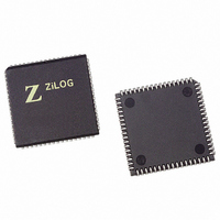
Z16C3516VSG Zilog, Z16C3516VSG Datasheet - Page 19

Z16C3516VSG
Manufacturer Part Number
Z16C3516VSG
Description
IC 16MHZ Z8500 CMOS ISCC 68-PLCC
Manufacturer
Zilog
Series
IUSC™r
Specifications of Z16C3516VSG
Controller Type
Serial Communications Controller (SCC)
Interface
USB
Voltage - Supply
4.75 V ~ 5.25 V
Current - Supply
50mA
Operating Temperature
0°C ~ 70°C
Mounting Type
Surface Mount
Package / Case
68-LCC (J-Lead)
Lead Free Status / RoHS Status
Lead free / RoHS Compliant
Other names
269-4690-5
Z16C3516VSG
Z16C3516VSG
Available stocks
Company
Part Number
Manufacturer
Quantity
Price
Company:
Part Number:
Z16C3516VSG
Manufacturer:
INTEL
Quantity:
6 219
- Current page: 19 of 268
- Download datasheet (3Mb)
UM011001-0601
2.4.6 DMA Register Access, Non-Multiplexed
Bus Mode
The registers in the DMA cell in the non-multiplexed bus
mode are accessed in a two-step process, using a Regis-
ter Pointer to perform the addressing. To access a partic-
ular register, the pointer bits must be set by writing to the
Channel Command /Address Register bits 4 through 0. Af-
ter the pointer bits are set, the next read or write cycle to
the DMA cell will access the desired register. At the con-
clusion of this read or write cycle, the pointer bits are reset
to “0s,” so that the next access will be to the Channel Com-
mand/Address Register.
The fact that the pointer bits are reset to “0,” unless explic-
itly set otherwise, means that the Channel Command/Ad-
dress Register may be accessed in a single cycle. That is,
it is not necessary to write the pointer bits with “0” before
accessing the Channel Command/Address Register. This
permits single access DMA enabling and resetting the
highest IUS through the encoded DMA Commands.
2.4.7 Notes on Pointer Accesses
The non-multiplexed bus accesses are accomplished as
described in the preceding paragraphs using the DMA
pointer for the DMA cell and the SCC cell pointer for
channels A and B. These two pointers are completely in-
dependent. If one of these pointers is written to with a
pointer value in preparation for a read or write to the se-
lected register, the pointer will hold its value until the cor-
responding cell is accessed. For example, suppose the
SCC cell pointer is written to in preparation to read an SCC
cell register in the next (or even subsequent) software pro-
gram steps. Before this SCC cell read takes place, a DMA
interrupt occurs and the program enters the interrupt ser-
vice routine prior to the SCC register read. In the interrupt
service routine, several DMA register accesses are made.
When the program exits the interrupt service routine and
returns to the interrupted process, the register access to
the SCC cell register proceeds correctly; the pointer was
left unaltered. A converse situation is true for the DMA cell.
It should be clear, however, that if an interrupt routine is in-
voked between the pointer write and the register access,
there can be conflict if the same cell is accessed in the in-
terrupt service routine. Assume in the above example that
the interrupt service routine accesses the SCC cell also.
Since the pointer has already been written, a second write
(the one in the interrupt service routine) will not write to the
pointer in WR0 but will write to the pointed to register. Sub-
sequent register access will also be incorrect. This sug-
gests that the pointer write and subsequent register ac-
cess be an uninterruptable pair and that the SCC Cell and
DMA cell or the processor interrupts be disabled during the
register access sequence.
Z16C35 ISCC™ User’s Manual
Interfacing the ISCC™
2-9
2
Related parts for Z16C3516VSG
Image
Part Number
Description
Manufacturer
Datasheet
Request
R

Part Number:
Description:
CMOS ISCC INTEGRATED SERIAL COMMUNICATIONS CONTROLLER
Manufacturer:
ZILOG [Zilog, Inc.]
Datasheet:

Part Number:
Description:
Communication Controllers, ZILOG INTELLIGENT PERIPHERAL CONTROLLER (ZIP)
Manufacturer:
Zilog, Inc.
Datasheet:

Part Number:
Description:
KIT DEV FOR Z8 ENCORE 16K TO 64K
Manufacturer:
Zilog
Datasheet:

Part Number:
Description:
KIT DEV Z8 ENCORE XP 28-PIN
Manufacturer:
Zilog
Datasheet:

Part Number:
Description:
DEV KIT FOR Z8 ENCORE 8K/4K
Manufacturer:
Zilog
Datasheet:

Part Number:
Description:
KIT DEV Z8 ENCORE XP 28-PIN
Manufacturer:
Zilog
Datasheet:

Part Number:
Description:
DEV KIT FOR Z8 ENCORE 4K TO 8K
Manufacturer:
Zilog
Datasheet:

Part Number:
Description:
CMOS Z8 microcontroller. ROM 16 Kbytes, RAM 256 bytes, speed 16 MHz, 32 lines I/O, 3.0V to 5.5V
Manufacturer:
Zilog, Inc.
Datasheet:

Part Number:
Description:
Low-cost microcontroller. 512 bytes ROM, 61 bytes RAM, 8 MHz
Manufacturer:
Zilog, Inc.
Datasheet:

Part Number:
Description:
Z8 4K OTP Microcontroller
Manufacturer:
Zilog, Inc.
Datasheet:

Part Number:
Description:
CMOS SUPER8 ROMLESS MCU
Manufacturer:
Zilog, Inc.
Datasheet:

Part Number:
Description:
SL1866 CMOSZ8 OTP Microcontroller
Manufacturer:
Zilog, Inc.
Datasheet:

Part Number:
Description:
SL1866 CMOSZ8 OTP Microcontroller
Manufacturer:
Zilog, Inc.
Datasheet:

Part Number:
Description:
OTP (KB) = 1, RAM = 125, Speed = 12, I/O = 14, 8-bit Timers = 2, Comm Interfaces Other Features = Por, LV Protect, Voltage = 4.5-5.5V
Manufacturer:
Zilog, Inc.
Datasheet:


