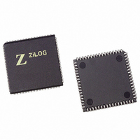
Z16C3516VSG Zilog, Z16C3516VSG Datasheet - Page 67

Z16C3516VSG
Manufacturer Part Number
Z16C3516VSG
Description
IC 16MHZ Z8500 CMOS ISCC 68-PLCC
Manufacturer
Zilog
Series
IUSC™r
Specifications of Z16C3516VSG
Controller Type
Serial Communications Controller (SCC)
Interface
USB
Voltage - Supply
4.75 V ~ 5.25 V
Current - Supply
50mA
Operating Temperature
0°C ~ 70°C
Mounting Type
Surface Mount
Package / Case
68-LCC (J-Lead)
Lead Free Status / RoHS Status
Lead free / RoHS Compliant
Other names
269-4690-5
Z16C3516VSG
Z16C3516VSG
Available stocks
Company
Part Number
Manufacturer
Quantity
Price
Company:
Part Number:
Z16C3516VSG
Manufacturer:
INTEL
Quantity:
6 219
- Current page: 67 of 268
- Download datasheet (3Mb)
UM011001-0601
Bit combination 11 programs Receive Interrupt on Special
Condition. This mode allows the receiver to interrupt only
on characters with a special receive condition. When an in-
terrupt occurs, the data containing the error is held in the
receive FIFO until an Error Reset command is issued.
When using this mode in conjunction with a DMA, the DMA
can be initialized and enabled before any characters have
been received by the SCC. This eliminates the time-critical
section of code required in the Receive Interrupt on First
Character or Special Condition mode; i.e. all data can be
transferred via the DMA so that the CPU need not handle
the first received character as a special case.
Bit 2 selects Parity Is Special Condition
If this bit is set to “1,” any received characters with parity
not matching the sense programmed in WR4 give rise to a
Special Receive Condition. If parity is disabled (WR4), this
bit is ignored. A special condition modifies the status of the
interrupt vector stored in WR2. During an interrupt ac-
knowledge cycle, this vector can be placed on the data
bus.
Write Register 2
D7
D6
D5 D4 D3 D2 D1 D0
Figure 5-4. Write Register 2
P R E L I M I N A R Y
Bit 1 is the Transmitter Interrupt Enable
If this bit is set to “1,” the transmitter requests an interrupt
whenever the transmit buffer becomes empty.
Bit 0 is the External/Status Master Interrupt Enable
This bit is the master enable for External/Status interrupts
including /DCD, /CTS, /SYNC pins, break, abort, the be-
ginning of CRC transmission when the Transmit/Under-
run/EOM latch is set, or when the counter in the baud rate
generator reaches “0.” Write Register 15 contains the indi-
vidual enable bits for each of these sources of Exter-
nal/Status interrupts. This bit is reset by a channel or hard-
ware reset.
5.4.3 Write Register 2 (Interrupt Vector)
WR2 is the interrupt vector register. Only one vector regis-
ter exists in the SCC cell, but it can be accessed through
either channel. The interrupt vector can be modified by sta-
tus information. This is controlled by the Vector Includes
Status (VIS) and the Status High/Status Low bits in WR9.
The bit positions for WR2 are shown in Figure 5-4. Note
that the DMA cell has its own interrupt vector register.
V0
V1
V2
V3
V4
V5
V6
V7
Interrupt
Vector
Z16C35ISCC™ User’s Manual
Register Descriptions
5-7
5
Related parts for Z16C3516VSG
Image
Part Number
Description
Manufacturer
Datasheet
Request
R

Part Number:
Description:
CMOS ISCC INTEGRATED SERIAL COMMUNICATIONS CONTROLLER
Manufacturer:
ZILOG [Zilog, Inc.]
Datasheet:

Part Number:
Description:
Communication Controllers, ZILOG INTELLIGENT PERIPHERAL CONTROLLER (ZIP)
Manufacturer:
Zilog, Inc.
Datasheet:

Part Number:
Description:
KIT DEV FOR Z8 ENCORE 16K TO 64K
Manufacturer:
Zilog
Datasheet:

Part Number:
Description:
KIT DEV Z8 ENCORE XP 28-PIN
Manufacturer:
Zilog
Datasheet:

Part Number:
Description:
DEV KIT FOR Z8 ENCORE 8K/4K
Manufacturer:
Zilog
Datasheet:

Part Number:
Description:
KIT DEV Z8 ENCORE XP 28-PIN
Manufacturer:
Zilog
Datasheet:

Part Number:
Description:
DEV KIT FOR Z8 ENCORE 4K TO 8K
Manufacturer:
Zilog
Datasheet:

Part Number:
Description:
CMOS Z8 microcontroller. ROM 16 Kbytes, RAM 256 bytes, speed 16 MHz, 32 lines I/O, 3.0V to 5.5V
Manufacturer:
Zilog, Inc.
Datasheet:

Part Number:
Description:
Low-cost microcontroller. 512 bytes ROM, 61 bytes RAM, 8 MHz
Manufacturer:
Zilog, Inc.
Datasheet:

Part Number:
Description:
Z8 4K OTP Microcontroller
Manufacturer:
Zilog, Inc.
Datasheet:

Part Number:
Description:
CMOS SUPER8 ROMLESS MCU
Manufacturer:
Zilog, Inc.
Datasheet:

Part Number:
Description:
SL1866 CMOSZ8 OTP Microcontroller
Manufacturer:
Zilog, Inc.
Datasheet:

Part Number:
Description:
SL1866 CMOSZ8 OTP Microcontroller
Manufacturer:
Zilog, Inc.
Datasheet:

Part Number:
Description:
OTP (KB) = 1, RAM = 125, Speed = 12, I/O = 14, 8-bit Timers = 2, Comm Interfaces Other Features = Por, LV Protect, Voltage = 4.5-5.5V
Manufacturer:
Zilog, Inc.
Datasheet:


