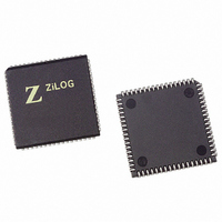
Z16C3516VSG Zilog, Z16C3516VSG Datasheet - Page 16

Z16C3516VSG
Manufacturer Part Number
Z16C3516VSG
Description
IC 16MHZ Z8500 CMOS ISCC 68-PLCC
Manufacturer
Zilog
Series
IUSC™r
Specifications of Z16C3516VSG
Controller Type
Serial Communications Controller (SCC)
Interface
USB
Voltage - Supply
4.75 V ~ 5.25 V
Current - Supply
50mA
Operating Temperature
0°C ~ 70°C
Mounting Type
Surface Mount
Package / Case
68-LCC (J-Lead)
Lead Free Status / RoHS Status
Lead free / RoHS Compliant
Other names
269-4690-5
Z16C3516VSG
Z16C3516VSG
Available stocks
Company
Part Number
Manufacturer
Quantity
Price
Company:
Part Number:
Z16C3516VSG
Manufacturer:
INTEL
Quantity:
6 219
- Current page: 16 of 268
- Download datasheet (3Mb)
Z16C35 ISCC™ User’s Manual
Interfacing the ISCC™
2.4 REGISTER ACCESS (Continued)
Address
AD4-AD0
00000
00001
00010
00011
00100
00101
00110
00111
01000
01001
01010
01011
01100
01101
01110
01111
10000
10001
10010
10011
10100
10101
10110
10111
11000
11001
11010
11011
11100
11101
11110
11111
2-6
Table 2-3. SCC Cell Address Map,
Multiplexed Bus Mode, Shift Right
Write
WR0B
WR0A
WR1B
WR1A
WR2
WR2
WR3B
WR3A
WR4B
WR4A
WR5B
WR5A
WR6B
WR6A
WR7B
WR7A
WR8B
WR8A
WR9
WR9
WR10B
WR10A
WR11B
WR11A
WR12B
WR12A
WR13B
WR13A
WR14B
WR14A
WR15B
WR15A
Read
RR0B
RR0A
RR1B
RR1A
RR2B
RR2A
RR3B
RR3A
RR0B
RR0A
(RR1B)
(RR1A)
RR2B
RR2A
(RR3B)
(RR3A)
RR8B
RR8A
(RR13B)
(RR13A)
RR10B
RR10A
(RR15B)
(RR15A)
RR12B
RR12A
RR13B
RR13A
(RR10B)
(RR10A)
RR15B
RR15A
2.4.2 SCC Cell Register Access,
Non-Multiplexed Bus
The registers in the SCC cell in the non-multiplexed bus
mode are accessed in a two-step process, using a Regis-
ter Pointer to perform the addressing. To access a partic-
ular register, the pointer bits must be set by writing to WR0
bits 2, 1, and 0 and, if required, using the Point High com-
mand to extend the three bit pointer to registers 8 through
15. This write to WR0 to set the pointer bits may be done
in either channel. There is only one pointer register and it
is used for both A and B channels. After the pointer bits are
set, the next read or write cycle to the SCC cell will access
the desired register in the channel selected during this
read or write cycle. At the conclusion of this read or write
cycle, the pointer bits are reset to “0s,” so that the next ac-
cess will be to WR0.
The fact that the pointer bits are reset to “0,” unless explic-
itly set otherwise, means that WR0 and RR0 may also be
accessed in a single cycle. That is, it is not necessary to
write the pointer bits with “0” before accessing WR0 or
RR0. There are three pointer bits in WR0, and these allow
access to the registers with addresses 0 through 7. Note
that a command may be written to WR0 at the same time
that the pointer bits are written.
To access the registers with addresses 8 through 15, a
special command must accompany the pointer bits;
WR0(4-3)=001. This precludes concurrently issuing a
command when pointing to these registers. The register
map for the ISCC in the non-multiplexed bus mode is
shown in Table 2-4 below. If, for some reason, the state of
the pointer bits is unknown, they may be reset to “0” by
performing a read cycle of the SCC cell. Once the pointer
bits have been set, the desired channel is selected by the
state of the A1/A//B pin during the actual read or write of
the desired SCC cell register.)
UM011001-0601
Related parts for Z16C3516VSG
Image
Part Number
Description
Manufacturer
Datasheet
Request
R

Part Number:
Description:
CMOS ISCC INTEGRATED SERIAL COMMUNICATIONS CONTROLLER
Manufacturer:
ZILOG [Zilog, Inc.]
Datasheet:

Part Number:
Description:
Communication Controllers, ZILOG INTELLIGENT PERIPHERAL CONTROLLER (ZIP)
Manufacturer:
Zilog, Inc.
Datasheet:

Part Number:
Description:
KIT DEV FOR Z8 ENCORE 16K TO 64K
Manufacturer:
Zilog
Datasheet:

Part Number:
Description:
KIT DEV Z8 ENCORE XP 28-PIN
Manufacturer:
Zilog
Datasheet:

Part Number:
Description:
DEV KIT FOR Z8 ENCORE 8K/4K
Manufacturer:
Zilog
Datasheet:

Part Number:
Description:
KIT DEV Z8 ENCORE XP 28-PIN
Manufacturer:
Zilog
Datasheet:

Part Number:
Description:
DEV KIT FOR Z8 ENCORE 4K TO 8K
Manufacturer:
Zilog
Datasheet:

Part Number:
Description:
CMOS Z8 microcontroller. ROM 16 Kbytes, RAM 256 bytes, speed 16 MHz, 32 lines I/O, 3.0V to 5.5V
Manufacturer:
Zilog, Inc.
Datasheet:

Part Number:
Description:
Low-cost microcontroller. 512 bytes ROM, 61 bytes RAM, 8 MHz
Manufacturer:
Zilog, Inc.
Datasheet:

Part Number:
Description:
Z8 4K OTP Microcontroller
Manufacturer:
Zilog, Inc.
Datasheet:

Part Number:
Description:
CMOS SUPER8 ROMLESS MCU
Manufacturer:
Zilog, Inc.
Datasheet:

Part Number:
Description:
SL1866 CMOSZ8 OTP Microcontroller
Manufacturer:
Zilog, Inc.
Datasheet:

Part Number:
Description:
SL1866 CMOSZ8 OTP Microcontroller
Manufacturer:
Zilog, Inc.
Datasheet:

Part Number:
Description:
OTP (KB) = 1, RAM = 125, Speed = 12, I/O = 14, 8-bit Timers = 2, Comm Interfaces Other Features = Por, LV Protect, Voltage = 4.5-5.5V
Manufacturer:
Zilog, Inc.
Datasheet:


