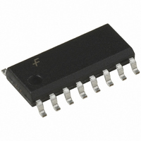
CD4053BCM Fairchild Semiconductor, CD4053BCM Datasheet - Page 7

CD4053BCM
Manufacturer Part Number
CD4053BCM
Description
IC MUX/DEMUX TRIPLE 2X1 16SOIC
Manufacturer
Fairchild Semiconductor
Series
4000Br
Datasheet
1.CD4053BCN.pdf
(13 pages)
Specifications of CD4053BCM
Function
Multiplexer/Demultiplexer
Circuit
3 x 2:1
On-state Resistance
240 Ohm
Voltage Supply Source
Dual Supply
Voltage - Supply, Single/dual (±)
±5 V ~ 15 V
Current - Supply
20µA
Operating Temperature
-55°C ~ 125°C
Mounting Type
Surface Mount
Package / Case
16-SOIC (0.154", 3.90mm Width)
Number Of Channels
3 Channel
On Resistance (max)
1050 Ohms
Propagation Delay Time
55 ns
On Time (max)
1200 ns
Off Time (max)
420 ns
Supply Voltage (max)
15 V
Supply Voltage (min)
5 V
Maximum Power Dissipation
500 mW
Maximum Operating Temperature
+ 125 C
Minimum Operating Temperature
- 55 C
Mounting Style
SMD/SMT
Number Of Switches
3
Lead Free Status / RoHS Status
Lead free / RoHS Compliant
Available stocks
Company
Part Number
Manufacturer
Quantity
Price
Company:
Part Number:
CD4053BCM
Manufacturer:
National
Quantity:
432
Part Number:
CD4053BCM
Manufacturer:
FAIRCHILD/仙童
Quantity:
20 000
Company:
Part Number:
CD4053BCMX
Manufacturer:
BOURNS
Quantity:
12 000
Part Number:
CD4053BCMX
Manufacturer:
FSC
Quantity:
20 000
t
t
t
t
C
C
C
C
Signal Inputs (V
t
t
Control Inputs, A, B, C and Inhibit
t
t
PZH,
PZL
PHZ,
PLZ
PHL
PLH
PHL,
PLH
AC Electrical Characteristics
T
Note 3: AC Parameters are guaranteed by DC correlated testing.
Note 4: A, B are two arbitrary channels with A turned “ON” and B “OFF”.
IN
OUT
IOS
PD
Symbol
A
25 C, t
Propagation Delay Time from
Inhibit to Signal Output
(channel turning on)
Propagation Delay Time from
Inhibit to Signal Output
(channel turning off)
Input Capacitance
Output Capacitance
(common OUT/IN)
Feedthrough Capacitance
Power Dissipation Capacitance
Sine Wave Response
(Distortion)
Frequency Response, Channel
“ON” (Sine Wave Input)
Feedthrough, Channel “OFF”
Crosstalk Between Any Two
Channels (frequency at 40 dB)
Propagation Delay Signal
Input to Signal Output
Control Input to Signal
Crosstalk
Propagation Delay Time from
Address to Signal Output
(channels “ON” or “OFF”)
r
Control input
Signal Input (IN/OUT)
CD4051
CD4052
CD4053
CD4051
CD4052
CD4053
IS
t
) and Outputs (V
f
20 ns, unless otherwise specified.
Parameter
OS
)
V
R
C
V
R
C
V
R
f
V
V
R
20 log
R
20 log
R
20 log
V
C
V
of channel.
Input Square Wave Amplitude
V
C
IS
EE
L
L
EE
L
L
EE
L
IS
EE
L
L
L
EE
L
EE
EE
L
1 kHz
1 k
50 pF
1 k
50 pF
10 k
1 k , V
1 k , V
1 k , V
50 pF
50 pF
5 V
V
V
V
V
10
10
10
V
V
V
SS
SS
SS
SI
SS
SS
SS
V
V
V
p-p
OS
OS
OS
0V
0V
0V
0V
EE
EE
EE
0V
0V, R
0V
/V
/V
(B)/V
(Note 3)
Conditions
IS
IS
0V, V
V
V
IS
L
SS
SS
(A)
3 dB
40 dB
10 k at both ends
IS
0V, V
0V, V
7
40 dB (Note 4)
5V
IS
IS
p-p
(A)
,
10V
5V
p-p
5V
,
p-p
V
10V
15V
10V
15V
10V
10V
10V
10V
10V
10V
10V
10V
15V
10V
10V
15V
5V
5V
5V
5V
DD
Min
0.04
Typ
600
225
160
210
100
110
140
500
180
120
0.2
75
10
30
15
70
40
10
25
15
10
65
5
8
3
www.fairchildsemi.com
1200
1000
Max
450
320
420
200
150
360
240
7.5
15
55
35
25
mV (peak)
Units
MHz
MHz
MHz
ns
ns
ns
ns
ns
ns
pF
pF
pF
pF
pF
pF
pF
pF
pF
ns
ns
ns
ns
ns
ns
%


