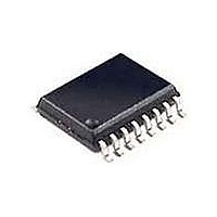
FAN9611MX Fairchild Semiconductor, FAN9611MX Datasheet - Page 18

FAN9611MX
Manufacturer Part Number
FAN9611MX
Description
Power Factor Correction ICs Interleaved Dual BCM PFC Controller
Manufacturer
Fairchild Semiconductor
Datasheet
1.FAN9611MX.pdf
(37 pages)
Specifications of FAN9611MX
Switching Frequency
525 KHz
Maximum Operating Temperature
+ 125 C
Mounting Style
SMD/SMT
Package / Case
SOIC-16
Minimum Operating Temperature
- 40 C
Lead Free Status / Rohs Status
Details
Available stocks
Company
Part Number
Manufacturer
Quantity
Price
Part Number:
FAN9611MX
Manufacturer:
FAIRCHILD/仙童
Quantity:
20 000
© 2008 Fairchild Semiconductor Corporation
FAN9611 / FAN9612 • Rev. 1.1.3
Application Information
1. Synchronization and Timing Functions
The
synchronization sub-system. At the heart of the system
is a dual-channel switching-frequency detector that
measures the switching period of each channel in every
switching cycle and locks their operating phase 180
degrees out of phase from each other. The slower
operating frequency channel is dominant, but there is no
master-slave arrangement. Moreover, as the frequency
constantly changes due to the varying input voltage,
either channel can be the slower dominant channel.
As opposed to the most common technique, where the
phase relationship between the channels is provided by
changing the on-time of one of the MOSFETs, the
FAN9611/12 controls the phase relationship by inserting
a turn-on delay before the next switching period starts
for the faster running phase. As shown in the
literature
stable under all operating conditions, while the off-time
modulation (or delaying the turn-on) is unconditionally
stable under all operating conditions.
a.
The restart timer is an integral part of the Sync-Lock™
synchronizing circuit. It ensures exact 180-degree out-
of-phase operation in restart timer operation. This is an
important safety feature. In the case of a non-operating
phase due to no ZCD detection, missing gate drive
connection (for example no gate resistor), one of the
power components failing in an open circuit, or similar
errors, the other phase is locked into restart timer
operation, preventing it from trying to deliver full power
to the load. This is called the dead-phase detect
protection.
The restart timer is set to approximately 16.5kHz, just
above the audible frequency range, to avoid any
acoustic noise generation.
b.
Just as the restart timer, the frequency clamp is
integrated into the synchronization and ensures exact
180-degree out-of-phase operation when the operating
frequency is limited. This might occur at very light-load
operation or near the zero crossing region of the line
voltage waveform. Limiting the switching frequency at
light load can improve efficiency, but has a negative
effect on power factor since the converter also enters
true DCM operation. The frequency clamp is set to
approximately 525kHz.
Restart Timer and Dead-Phase Detect
Protection
Frequency Clamp
FAN9611/12
[1]
, the on-time modulation technique is not
employs
a
sophisticated
18
2. FAN9612 Startup with 12V Bias (Less than
The FAN9612 (not FAN9611) is designed so that the
controller can start even if the auxiliary bias voltage is
less than the controller’s under-voltage lockout start
threshold. This is useful if the auxiliary power is 12V or
below. This configuration also allows bias power
designs using a bootstrap winding to start the FAN9612
without a dedicated startup resistor.
In the boost PFC topology, the output voltage is pre-
charged to the peak line voltage by the boost diode. As
soon as voltage is present at the output of the boost
converter, current starts to flow through the feedback
resistors from the boost output to GND. Using an
external low-voltage MOSFET in series with the lower
resistor in the feedback divider, as shown in Figure 27;
this current can be diverted to charge the V
capacitor of the controller. The upper resistor becomes
a current source to charge the capacitor. To accomplish
this, a small external diode should be connected
between the VDD and FB pins.
As V
the IC, the 5V reference is turned on, which turns on the
external MOSFET and connects the resistor of the
feedback divider to ground. The IC checks if the FB
voltage is below 3.22V, ensuring that the FB pin is in its
normal operating voltage range, before enabling the rest
of the IC operation. The diode between the FB pin and
the VDD pin is reverse biased and the FB pin reverts to
its normal role of output voltage sensing. A simplified
circuit implementation for this proprietary startup method
is shown in Figure 27.
If, for whatever reason, the bias to the IC drops below
the under-voltage lockout level, the startup process is
repeated.
Figure 27. Simplified FAN9612 Startup Circuit Using
UVLO)
DD
the Output Feedback Resistors to Provide a
rises past the under-voltage lockout threshold of
Charging Current
www.fairchildsemi.com
DD
bypass


