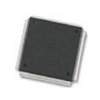
MC68376BAMFT20 Freescale Semiconductor, MC68376BAMFT20 Datasheet - Page 104

MC68376BAMFT20
Manufacturer Part Number
MC68376BAMFT20
Description
Manufacturer
Freescale Semiconductor
Datasheet
1.MC68376BAMFT20.pdf
(434 pages)
Specifications of MC68376BAMFT20
Cpu Family
68K/M683xx
Device Core
ColdFire
Device Core Size
32b
Frequency (max)
20MHz
Interface Type
QSPI/SCI
Program Memory Type
ROM
Program Memory Size
8KB
Total Internal Ram Size
7.5KB
# I/os (max)
18
Number Of Timers - General Purpose
2
Operating Supply Voltage (typ)
5V
Operating Supply Voltage (max)
5.25V
Operating Supply Voltage (min)
4.75V
On-chip Adc
16-chx10-bit
Instruction Set Architecture
RISC
Operating Temp Range
-40C to 125C
Operating Temperature Classification
Automotive
Mounting
Surface Mount
Pin Count
160
Package Type
PQFP
Lead Free Status / Rohs Status
Not Compliant
Available stocks
Company
Part Number
Manufacturer
Quantity
Price
Company:
Part Number:
MC68376BAMFT20
Manufacturer:
FREESCAL
Quantity:
245
- Current page: 104 of 434
- Download datasheet (7Mb)
5.5.5 Operand Transfer Cases
5.6 Bus Operation
5.6.1 Synchronization to CLKOUT
5-26
MOTOROLA
Current
Cycle
NOTES:
Table 5-12 is a summary of how operands are aligned for various types of transfers.
OPn entries are portions of a requested operand that are read or written during a bus
cycle and are defined by SIZ1, SIZ0, and ADDR0 for that bus cycle. The following
paragraphs discuss all the allowable transfer cases in detail.
Internal microcontroller modules are typically accessed in two system clock cycles.
Regular external bus cycles use handshaking between the MCU and external periph-
erals to manage transfer size and data. These accesses take three system clock cy-
cles, with no wait states. During regular cycles, wait states can be inserted as needed
by bus control logic. Refer to 5.6.2 Regular Bus Cycles for more information.
Fast termination cycles, which are two-cycle external accesses with no wait states,
use chip-select logic to generate handshaking signals internally. Chip-select logic can
also be used to insert wait states before internal generation of handshaking signals.
Refer to 5.6.3 Fast Termination Cycles and 5.9 Chip-Selects for more information.
Bus control signal timing, as well as chip-select signal timing, are specified in APPEN-
DIX A ELECTRICAL CHARACTERISTICS. Refer to the SIM Reference Manual (SIM-
RM/AD) for more information about each type of bus cycle.
External devices connected to the MCU bus can operate at a clock frequency different
from the frequencies of the MCU as long as the external devices satisfy the interface
signal timing constraints. Although bus cycles are classified as asynchronous, they are
interpreted relative to the MCU system clock output (CLKOUT).
Descriptions are made in terms of individual system clock states, labeled {S0, S1,
S2,..., S
not correspond to any implemented machine state. A clock cycle consists of two suc-
cessive states. Refer to Table A-4 for more information.
1
2
3
4
5
6
7
8
9
1. All transfers are aligned. The CPU32 does not support misaligned word or long-word transfers.
2. Operands in parentheses are ignored by the CPU32 during read cycles.
3. Three-Byte transfer cases occur only as a result of a long word to 8-bit port transfer.
Byte to 8-bit port (even)
Byte to 8-bit port (odd)
Byte to 16-bit port (even)
Byte to 16-bit port (odd)
Word to 8-bit port
Word to 16-bit port
3-Byte to 8-bit port
Long word to 8-bit port
Long word to 16-bit port
N
Transfer Case
}. The designation “state” refers to the logic level of the clock signal and does
3
1
Table 5-12 Operand Alignment
SYSTEM INTEGRATION MODULE
SIZ1
0
1
1
1
0
0
0
0
0
SIZ0
1
1
1
1
0
0
1
0
0
ADDR0 DSACK1 DSACK0
0
1
0
1
0
0
1
0
0
1
1
0
0
1
0
1
1
0
0
0
1
1
0
1
0
0
1
DATA
[15:8]
(OP0)
OP0
OP0
OP0
OP0
OP0
OP0
OP0
OP0
USER’S MANUAL
(OP0)
DATA
(OP0)
(OP0)
(OP1)
(OP0)
(OP0)
[7:0]
OP0
OP1
OP1
MC68336/376
2
Cycle
Next
—
—
—
—
—
2
5
7
6
Related parts for MC68376BAMFT20
Image
Part Number
Description
Manufacturer
Datasheet
Request
R
Part Number:
Description:
Manufacturer:
Freescale Semiconductor, Inc
Datasheet:
Part Number:
Description:
Manufacturer:
Freescale Semiconductor, Inc
Datasheet:
Part Number:
Description:
Manufacturer:
Freescale Semiconductor, Inc
Datasheet:
Part Number:
Description:
Manufacturer:
Freescale Semiconductor, Inc
Datasheet:
Part Number:
Description:
Manufacturer:
Freescale Semiconductor, Inc
Datasheet:
Part Number:
Description:
Manufacturer:
Freescale Semiconductor, Inc
Datasheet:
Part Number:
Description:
Manufacturer:
Freescale Semiconductor, Inc
Datasheet:
Part Number:
Description:
Manufacturer:
Freescale Semiconductor, Inc
Datasheet:
Part Number:
Description:
Manufacturer:
Freescale Semiconductor, Inc
Datasheet:
Part Number:
Description:
Manufacturer:
Freescale Semiconductor, Inc
Datasheet:
Part Number:
Description:
Manufacturer:
Freescale Semiconductor, Inc
Datasheet:
Part Number:
Description:
Manufacturer:
Freescale Semiconductor, Inc
Datasheet:
Part Number:
Description:
Manufacturer:
Freescale Semiconductor, Inc
Datasheet:
Part Number:
Description:
Manufacturer:
Freescale Semiconductor, Inc
Datasheet:
Part Number:
Description:
Manufacturer:
Freescale Semiconductor, Inc
Datasheet:


