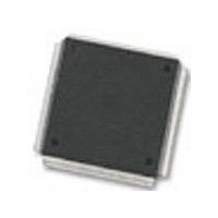
MC68376BAMFT20 Freescale Semiconductor, MC68376BAMFT20 Datasheet - Page 74

MC68376BAMFT20
Manufacturer Part Number
MC68376BAMFT20
Description
Manufacturer
Freescale Semiconductor
Datasheet
1.MC68376BAMFT20.pdf
(434 pages)
Specifications of MC68376BAMFT20
Cpu Family
68K/M683xx
Device Core
ColdFire
Device Core Size
32b
Frequency (max)
20MHz
Interface Type
QSPI/SCI
Program Memory Type
ROM
Program Memory Size
8KB
Total Internal Ram Size
7.5KB
# I/os (max)
18
Number Of Timers - General Purpose
2
Operating Supply Voltage (typ)
5V
Operating Supply Voltage (max)
5.25V
Operating Supply Voltage (min)
4.75V
On-chip Adc
16-chx10-bit
Instruction Set Architecture
RISC
Operating Temp Range
-40C to 125C
Operating Temperature Classification
Automotive
Mounting
Surface Mount
Pin Count
160
Package Type
PQFP
Lead Free Status / Rohs Status
Not Compliant
Available stocks
Company
Part Number
Manufacturer
Quantity
Price
Company:
Part Number:
MC68376BAMFT20
Manufacturer:
FREESCAL
Quantity:
245
- Current page: 74 of 434
- Download datasheet (7Mb)
4.10.7 Background Mode Registers
4.10.7.1 Fault Address Register (FAR)
4.10.7.2 Return Program Counter (RPC)
4-22
MOTOROLA
BDM processing uses three special purpose registers to keep track of program context
during development. A description of each follows.
The FAR contains the address of the faulting bus cycle immediately following a bus or
address error. This address remains available until overwritten by a subsequent bus
cycle. Following a double bus fault, the FAR contains the address of the last bus cycle.
The address of the first fault (if there was one) is not visible to the user.
The RPC points to the location where fetching will commence after transition from
background mode to normal mode. This register should be accessed to change the
flow of a program under development. Changing the RPC to an odd value will cause
an address error when normal mode prefetching begins.
Read Memory Location
Write Memory Location
Read System Register
Write System Register
Dump Memory Block
Read D/A Register
Resume Execution
Write D/A Register
Reset Peripherals
Fill Memory Block
Patch User Code
No Operation
Command
Table 4-6 Background Mode Command Summary
WDREG/WAREG
RDREG/RAREG
Mnemonic
WSREG
RSREG
WRITE
DUMP
CENTRAL PROCESSOR UNIT
READ
CALL
NOP
FILL
RST
GO
Read the selected address or data register and return the
results via the serial interface.
The data operand is written to the specified address or data
register.
The specified system control register is read. All registers that
can be read in supervisor mode can be read in background
mode.
The operand data is written into the specified system control
register.
Read the sized data at the memory location specified by the
long-word address. The source function code register (SFC)
determines the address space accessed.
Write the operand data to the memory location specified by the
long-word address. The destination function code (DFC) reg-
ister determines the address space accessed.
Used in conjunction with the READ command to dump large
blocks of memory. An initial READ is executed to set up the
starting address of the block and retrieve the first result. Sub-
sequent operands are retrieved with the DUMP command.
Used in conjunction with the WRITE command to fill large
blocks of memory. An initial WRITE is executed to set up the
starting address of the block and supply the first operand. Sub-
sequent operands are written with the FILL command.
The pipe is flushed and re-filled before resuming instruction
execution at the current PC.
Current program counter is stacked at the location of the cur-
rent stack pointer. Instruction execution begins at user patch
code.
Asserts RESET for 512 clock cycles. The CPU is not reset by
this command. Synonymous with the CPU RESET instruction.
NOP performs no operation and may be used as a null com-
mand.
Description
USER’S MANUAL
MC68336/376
Related parts for MC68376BAMFT20
Image
Part Number
Description
Manufacturer
Datasheet
Request
R
Part Number:
Description:
Manufacturer:
Freescale Semiconductor, Inc
Datasheet:
Part Number:
Description:
Manufacturer:
Freescale Semiconductor, Inc
Datasheet:
Part Number:
Description:
Manufacturer:
Freescale Semiconductor, Inc
Datasheet:
Part Number:
Description:
Manufacturer:
Freescale Semiconductor, Inc
Datasheet:
Part Number:
Description:
Manufacturer:
Freescale Semiconductor, Inc
Datasheet:
Part Number:
Description:
Manufacturer:
Freescale Semiconductor, Inc
Datasheet:
Part Number:
Description:
Manufacturer:
Freescale Semiconductor, Inc
Datasheet:
Part Number:
Description:
Manufacturer:
Freescale Semiconductor, Inc
Datasheet:
Part Number:
Description:
Manufacturer:
Freescale Semiconductor, Inc
Datasheet:
Part Number:
Description:
Manufacturer:
Freescale Semiconductor, Inc
Datasheet:
Part Number:
Description:
Manufacturer:
Freescale Semiconductor, Inc
Datasheet:
Part Number:
Description:
Manufacturer:
Freescale Semiconductor, Inc
Datasheet:
Part Number:
Description:
Manufacturer:
Freescale Semiconductor, Inc
Datasheet:
Part Number:
Description:
Manufacturer:
Freescale Semiconductor, Inc
Datasheet:
Part Number:
Description:
Manufacturer:
Freescale Semiconductor, Inc
Datasheet:


