PSB 2132 H V2.2 Infineon Technologies, PSB 2132 H V2.2 Datasheet
PSB 2132 H V2.2
Specifications of PSB 2132 H V2.2
SP000007696


Related parts for PSB 2132 H V2.2

PSB 2132 H V2.2 Summary of contents
Page 1
Hard fer enc e Manual , eb. 2001 ® ...
Page 2
... Infineon Technologies Office. Infineon Technologies Components may only be used in life-support devices or systems with the express written approval of Infineon Technologies failure of such components can reasonably be expected to cause the failure of that life-support device or system affect the safety or effectiveness of that device or system. Life support devices or systems are intended to be implanted in the human body support and/or maintain and sustain and/or protect human life ...
Page 3
Hard Ref er enc e M anual eb. 2001 ® ...
Page 4
... PSB 2132 Revision History: Previous Version: Page Subjects (major changes since last revision) For questions on technology, delivery and prices please contact the Infineon Technologies Offices in Germany or the Infineon Technologies Companies and Representatives worldwide: see our webpage at http://www.infineon.com/ ® ® ® ABM ...
Page 5
Table of Contents Preface ...
Page 6
Table of Contents 5.1.2 Analog Interface Pins . . . . . . . . . . . . . . . . . . . . . . . . . . . . . . . . . ...
Page 7
Table of Contents 9 Test Modes . . . . . . . . . . . . . . . . . . . . . . . . . . . . . . . . . . ...
Page 8
List of Figures ® Figure 1 SICOFI 2-TE Architecture . . . . . . . . . . . . . . . . . . . . . . . . . . . . . . . ...
Page 9
List of Tables Table 1 Pin Definitions and Functions . . . . . . . . . . . . . . . . . . . . . . . . . . . . . . . ...
Page 10
Preface This document provides detailed technical information about the SICOFI intended for anyone considering or using the device for system design or board layout for a broad range of analog telephony applications. Organization of this Document This Hardware Reference Manual ...
Page 11
Overview The two-channel codec filter PSB 2132 SICOFI which provides independent filter structures for both channels. Its analog I/O pins are used to connect to external subscriber line interface circuits (SLICs). Their signals are internally routed to the analog-to-digital ...
Page 12
Two Channel Codec Filter for Terminal Application ® SICOFI 2-TE Version 2.2 1.1 Features • Two-channel single chip codec with digital filters • High analog driving capability (300 , 50 pF) for direct driving of transformers • Digital Signal Processing ...
Page 13
Logic Symbol Channel Analog 1 Interface Channel 2 Channel 1 Signaling Interface Channel 2 ® Figure 2 SICOFI 2-TE Logic Symbol 1.3 Typical Applications Many applications will benefit from the versatility of the SICOFI The inherent flexibility enables several ...
Page 14
Pin Descriptions 2.1 Pin Diagram (top view IN1 GNDA1 OUT1 V 52 DDA12 V 53 OUT2 GNDA2 54 ...
Page 15
Pin Definitions and Functions Table 1 Pin Definitions and Functions Pin Symbol Type Function 1, 2 NUI I Non Usable Input Pins must be tied directly to digital ground GNDD (Pin 21 NUIO I/O Non Usable Input/Output ...
Page 16
Pin Symbol Type Function 22 DCL I Master Clock Input 1536 kHz signal must be applied for any operation. DCL, BCL, and FSC must be synchronous. 23 RESET# I Reset Input Forces the device to default setting mode; active low. ...
Page 17
Pin Symbol Type Function 33 RGEN O Ring Generator Output Configurable output clock (2 … 28 ms) synchronous to DCL. Square-wave signal with duty cycle 1:1. 34 INT12 O Interrupt Output, Channels 1 and 2 Active high. 35 SI1_1 I ...
Page 18
Pin Symbol Type Function 54 GNDA2 I Analog Ground, Channel 2 Not internally connected to GNDD or GNDA1 or GNDA Analog Voice (Voltage) Input, Channel 2 IN2 Requires a coupling capacitor > the SLIC. V ...
Page 19
Functional Description ® The SICOFI 2-TE in combination with four Subscriber Line Interface Circuits (SLIC) provides four analog telephone lines. The SLIC can be either a transformer or an electronic circuit with operational amplifiers. It must have a defined ...
Page 20
PSB 2132, SICOFI2-TE V ADC Hardware IN1 Filters V DAC OUT1 V ADC Hardware IN2 Filters V DAC OUT2 DCL PLL, RGEN Clocking CHCLK SIx_y SOx_y Signaling Interface SBx_y INT12 ® Figure 4 SICOFI 2-TE Block Diagram Figure 4 shows ...
Page 21
Operational Description Each channel of the SICOFI “Operating”. These states can be switched by programming Bit 0 (PU) in the channel-specific configuration register CR1. “Standby” power-saving state. Keeping any unused channels in this state reduces the overall ...
Page 22
Hardware Reset Voltage levels lower than 1.2 V applied to Pin 23 (RESET#) for more than 3 µs will reset ® the SICOFI 2-TE. Spikes that are shorter than 1 µs will be ignored. When RESET# is ® released ...
Page 23
Table 4 Power Dissipation No. of Channels Operating None 1 2 4.2 Transmission Characteristics 4.2.1 Overload Point The overload point of the SICOFI amplitude of a sine wave level of 1.572 Vrms. Higher input signal levels will be distorted. Theoretical ...
Page 24
Compressor Gain Relative to Coding Law The µ-Law compressor unit of the SICOFI which has to be considered for the total gain calculation. The accumulated gain of all programmable transmit filters (AX1+AX2+FRX) must not exceed the ...
Page 25
Operating Conditions The figures in this document are based on the subscriber-line board requirements. Proper adjustment of the programmable filters (transhybrid balancing, impedance matching, frequency-response correction) requires a complete knowledge of the analog environment in which the SICOFI transmission ...
Page 26
Gain Accuracy Table 7 Gain Accuracy Parameter Symbol G Absolute Gain Variation with Temperature Variation with Supply Voltage Variation with Analog Gain 4.2.6 Gain Tracking (Receive and Transmit) The gain deviation for a 1014 Hz sine-wave input signal will ...
Page 27
Frequency Response Table 9 Attenuation with Frequency in Transmit and Receive Direction Receive Loss Input Frequency min 100 Hz 0 100 Hz to 200 Hz 0 200 Hz to 300 Hz -0.125 300 Hz to 3.0 ...
Page 28
Group Delay Distortion with Frequency The Group Delay Distortion in transmit and receive direction will stay within the limits shown in Table 11. Group Delay Distortion values are referenced to the minimum value of Group Delay (T min). G ...
Page 29
Harmonic and Intermodulation Distortion Table 14 Harmonic and Intermodulation Distortion Parameter Symbol Harmonic Distortion order Intermodulation R IMD 2 R IMD 3 4.2.11 Total Distortion Table 15 Signal-to-Total Distortion Ratio Measured with Sine ...
Page 30
Single Frequency Distortion Table 16 Single Frequency Distortion Test Input Signal Receive Direction Transmit Direction Any resulting signal with a frequency different from the test input signal will stay at least 28 dB below the input signal level. 4.2.13 ...
Page 31
Out-of-Band Discrimination in Transmit Direction With any 0 dBm0 sine-wave signal below 100 Hz and in the range from 3.4 kHz to 100 kHz (out-of-band signal) applied to an analog input (V frequency component at the digital output will ...
Page 32
Out-of-Band Discrimination in Receive Direction With any 0 dBm0 sine-wave frequency in the range from 300 Hz to 3.99 kHz applied to the digital input (DU or DD), the level of any resulting out-of-band signal at the analog output ...
Page 33
Figure 13 Analog Output: Out-of-Band Idle Channel Noise 4.2.18 Transhybrid Loss The quality of Transhybrid-Balancing is very sensitive to deviations in gain, group delay, and deviations inherent to ...
Page 34
Interface Description ® The SICOFI 2-TE provides four interfaces: • Analog Interface, • IOM-2 PCM Interface, • Signaling Interface, and • Serial Microcontroller Interface. A general description of these interface is given in the Product Overview, Chapter 4. Refer ...
Page 35
SLIC 1 > 39nF R Load µ Ext1 Figure 14 Analog Interface to Two Subscriber Line Interface Circuits (SLICs) ...
Page 36
Analog Interface Pins Table 21 Analog Interface Pins Symbol Pin V 49 Analog Input, Channel 1, 2 IN1 Requires a coupling capacitor > the SLIC, see Figure 14 IN2 V 51 Analog Output, Channel 1, ...
Page 37
IOM-2 PCM Interface Pins Table 22 IOM-2 PCM Interface Pins Symbol Pin Function DCL 22 Master Clock input, 1536 kHz. BCL 32 Bit Clock input at 768 kHz or 1536 kHz. FSC 31 Frame Synchronization Clock, 8 kHz. DD ...
Page 38
FSC DU/ MON0 ... DCL BCL DU/ Figure 15 IOM-2 PCM Interface Time Slot Positions 5.3 Signaling Interface ® The SICOFI 2-TE Signaling Interface is used to monitor and control supervision ...
Page 39
Signaling Interface Pins SLIC 1 RWG Input Tip Operating Mode Ring Off-Hook Det. Ground Key Det. Polarity Rev. Status LED Figure 16 Signaling Example: Two Subscriber Lines Table 24 Signaling Interface: Pins and Functions for SLIC Interfaces Table 25 ...
Page 40
Debouncing Functions and Interrupt Generation All signaling inputs are sampled at programmable intervals (Field N in register XR4). If all the inputs assigned to one channel-pair (1&2) have been stable for two subsequent samples their values are stored in ...
Page 41
SICOFI2-TE CS# DCLK DIN Out Out Microcontroller Configuration A: Separate DIN, DOUT Figure 17 Serial Microcontroller Interface 5.4.1 Serial Microcontroller Interface Pins Table 27 Serial Microcontroller Interface: Pins and Functions Symbol Pin Function CS# 17 Chip Select, enable to read ...
Page 42
CS# DCLK DIN Write Command DOUT Figure 18 Example for a Two-Byte Write Access 5.4.3 Read Access If the first eight bits received via DIN represent a read command, the SICOFI ...
Page 43
CS# DCLK DIN Read Command High 'Z' DOUT Figure 20 Example for a Read Access with Byte-by-Byte Transfer Read and write commands can be chained by leaving CS# low after the completion ...
Page 44
Programming Overview The transmission characteristics and interfaces of the PSB 2132 can be adapted to various environments. Configuring the functional blocks and programming the digital filter behavior is accomplished by loading values to the Configuration Registers and the Coefficient ...
Page 45
Register Maps Table 29 Read Access to Common Configuration Register (XR) Map Bit 7 Bit 6 XR0 0 0 XR1 0 0 XR2 0 0 XR3 0 0 XR4 Field N (Signal Debounce) XR5 0 0 XR6 C-Mode X-S ...
Page 46
CRAM Structure Coefficient RAM (CRAM) is used to store the individual coefficients calculated for each channel. The coefficients can be written and read through the Microcontroller Interface. The IM, FRX, FRR, AX, AR, TG1, TG2, and TH coefficients are ...
Page 47
Table 33 Coefficient RAM (CRAM) Structure per Set TH Part 1 TH Part 2 TH Part 3 6.2 Types of Commands and Data Bytes Coefficients and register contents are programmed and accessed through command sequences via the Microcontroller Interface. There ...
Page 48
Application Hints 7.1 Support Tools 7.1.1 Development Board The Evaluation Package EASY 2466 includes the following hardware: ® • One SICOFI 2-TE Evaluation Board STUT 2466 with connectors for four optional SLIC daughter cards and BNC connectors to a ...
Page 49
Guidelines for Board Design 7.2.1 Filter Capacitors • For high frequency noise rejection, use 100 nF SMD ceramic capacitors on pins and DDA12 DDA DDREF are recommended. • Use one 100 nF SMD ceramic capacitor ...
Page 50
Proposal for SICOFI For a new layout design it is recommended to use a separate ground-layer which gives the possibilty to connect all ground-pins of the SICOFI ohmic together. Furthermore, an optimum board layout should follow these recommendations • ...
Page 51
Electrical Characteristics and Timing Diagrams 8.1 Absolute Maximum Ratings Parameter V referred to GNDD DD GNDA to GNDD Analog input and output voltage V Referred Referred to GNDA = 0 V All digital input ...
Page 52
Operating Range 5%; GNDD = 0 V; GNDA = Parameter V supply current: DD Standby 1 channel operating 2 channels operating Power supply rejection ratio (either direction) 8.3 Digital Interface V = ...
Page 53
Analog Interface 5%; GNDD = 0 V; GNDA = Parameter Input resistance Output resistance Output load Input leakage current Input offset voltage Output offset voltage Input voltage range (AC) 8.4.1 Coupling Capacitors ...
Page 54
IOM-2 PCM-Interface Timing 8.6.1 Single Clocking Mode t BCL 50% BCL t t FSC_S FSC_H FSC t t DR_S DR_H DU/DD in DU/DD out Figure 26 PCM Interface Timing in Single Clocking Mode Parameter Period of BCL BCL high ...
Page 55
Double Clocking Mode t BCL 50% BCL t t FSC_H FSC_S FSC t t DR_S DR_H DU/DD in DU/DD out Figure 27 PCM Interface Timing in Double Clocking Mode Parameter Period of BCL BCL high time Period FSC FSC ...
Page 56
Microcontroller Interface Timing t DCLK 50% DCLK t CS_S CS DIN_S DIN_H DIN DOUT Figure 28 Timing of the Microcontroller Interface Parameter Period of DCLK DCLK high time CS# setup time CS# hold time DIN setup time ...
Page 57
Signaling Interface Timing 8.8.1 Timing from the Microcontroller Interface to the SO/SB-pins DCLK DIN SO/SB Output SB (Output Input) SB (Input Output) Figure 29 Signaling Output Timing (Data Downstream) Parameter Symbol 1) SO/SB delay time SB to "Z" - ...
Page 58
Test Modes ® Each SICOFI 2-TE channel has four test loops that feed the analog input signal back to the analog output (analog test loops), and five test loops that feed the PCM input signal back to the PCM ...
Page 59
Digital Loops The digital loops feed signals from the receive path back to the transmit path. There are five digital loops, which are shown in Figure 31. Analog AGX ADC Input IM2 Analog AGR DAC Output Figure 31 Digital ...
Page 60
Cut-Off’s The transmit path and the receive path can be cut off at two locations each. Figure 32 shows the locations in the signal paths. Analog AGX ADC Input IM2 COR4M Analog AGR DAC Output Figure 32 Cut-Off’s Table ...
Page 61
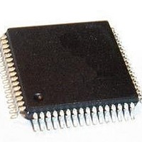
Package Outlines P-MQFP-64 (Plastic Metric Quad Flat Package) Sorts of Packing Package outlines for tubes, trays etc. are contained in our Data Book “Package Information”. SMD = Surface Mounted Device Hardware Reference Manual 52 PSB 2132 Package Outlines Dimensions ...
Page 62
Glossary AC ADC CMOS CRAM DAC DC DLC DSP DTMF FIR FTTC IIR IOM-2 ISDN ITU ITU-T NT PBX PCM POTS PSTN PTT QSICOS RITL RT SICOFI SLIC t/r TA Hardware Reference Manual Alternating Current Analog-to-Digital Converter Complementary Metal ...
Page 63
Index Symbols µ-Law . . . . . . . . . . . . . . . 2, 11, 14, 19, 27 µ-Law mode . . . . . . . . . . . . . . . ...
Page 64
Control data input/output pins Conversion utilities . . . . . . . . . . . . . . . . 39 COP . . . . . . . . ...
Page 65
FRR . . . . . . . . . . . . . . . . . . . . . . . . . . . 37 FRX ...
Page 66
Noise rejection . . . . . . . . . . . . . . . . . . . 40 Non usable input ...
Page 67
RST Sampling ...
Page 68
Transhybrid balancing . . . . 3, 10, 11, 16, 24 Transhybrid loss . . . . . . . . . . . . . . . . . . 24 Transmission characteristics . . . . 10, 14, ...
Page 69
... Better operating results and business excellence mean less idleness and wastefulness for all of us, more professional success, more accurate information, a better overview and, thereby, less frustration and more satisfaction.” Dr. Ulrich Schumacher Published by Infineon Technologies AG ...