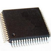
PSB 2132 H V2.2 Infineon Technologies, PSB 2132 H V2.2 Datasheet - Page 40

PSB 2132 H V2.2
Manufacturer Part Number
PSB 2132 H V2.2
Description
IC CODEC FILTER 2CHAN MQFP-64
Manufacturer
Infineon Technologies
Series
SICOFI®r
Datasheet
1.PSB_2132_H_V2.2.pdf
(69 pages)
Specifications of PSB 2132 H V2.2
Package / Case
64-QFP
Function
CODEC Filter
Interface
IOM-2 PCM, SPI
Number Of Circuits
2
Voltage - Supply
5V
Current - Supply
18mA
Power (watts)
90mW
Mounting Type
Surface Mount
Includes
Level Metering Function, Tone Generation
Number Of Adc Inputs
2
Number Of Dac Outputs
2
Interface Type
Serial
Operating Supply Voltage
5 V
Maximum Operating Temperature
+ 70 C
Mounting Style
SMD/SMT
Minimum Operating Temperature
0 C
Number Of Channels
2
Snr
35.4 dB
Supply Current
40 mA
Lead Free Status / RoHS Status
Lead free / RoHS Compliant
Operating Temperature
-
Lead Free Status / RoHS Status
Lead free / RoHS Compliant, Lead free / RoHS Compliant
Other names
PSB2132HV2.2XT
SP000007696
SP000007696
Hardware Reference Manual
5.3.2
All signaling inputs are sampled at programmable intervals (Field N in register XR4). If
all the inputs assigned to one channel-pair (1&2) have been stable for two subsequent
samples their values are stored in the signaling registers and the associated interrupt
output (INT12) is set high. The debouncing functions and interrupt generation require a
1536 kHz signal on Pin 22 (DCL). If, for power savings reasons, DCL is temporarily
disabled, a signaling change interrupt can be generated by external hardware. Refer to
the Programmer’s Reference Manual for further details on this function.
5.3.3
Two programmable Clock Output signals are provided by the PSB 2132:
• RGEN (Pin 33) divided by two can drive the ring input of a ringing SLIC. It is configured
• CHCLK (Pin 16) is configured in register XR5.CHCLK.
• CHCLK = 16,384 kHz: Requires at least one channel in POWER-UP state.
Table 26
5.4
The Serial Microcontroller Interface is used to access the SICOFI
registers and the Coefficient RAM (CRAM). The Serial Microcontroller Interface consists
of four pins: two data pins (DIN, DOUT), one clock pin (DCLK) and one pin for chip select
(CS#). If DIN and DOUT are strapped together, only three microcontroller I/O pins are
required to build this interface.
0001 to 1110
in register XR4.Field T.
XR4.Field T
0000
1111
Debouncing Functions and Interrupt Generation
Clock Output Signals
Serial Microcontroller Interface
Clock Programming
REGEN
(min. 2 ms, max. 28 ms)
Clock period = T *2ms
High level (+5V)
Output (Pin 33)
Low level (0V)
31
XR5.CHCLK
00
01
10
11
CHCLK
Interface Description
16,384 kHz signal
Output (Pin 16)
High level (+5V)
512 kHz signal
256 kHz signal
®
2-TE’s internal
PSB 2132
2001-02-20


