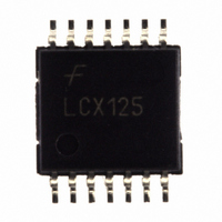
74LCX125MTC Fairchild Semiconductor, 74LCX125MTC Datasheet - Page 6
74LCX125MTC
Manufacturer Part Number
74LCX125MTC
Description
IC BUFFER QUAD LV N-INV 14TSSOP
Manufacturer
Fairchild Semiconductor
Series
74LCXr
Datasheet
1.74LCX125MX.pdf
(13 pages)
Specifications of 74LCX125MTC
Logic Type
Buffer/Line Driver, Non-Inverting
Number Of Elements
4
Number Of Bits Per Element
1
Current - Output High, Low
24mA, 24mA
Voltage - Supply
2 V ~ 3.6 V
Operating Temperature
-40°C ~ 85°C
Mounting Type
Surface Mount
Package / Case
14-TSSOP
Logic Family
74LCX
Number Of Channels Per Chip
Quad
Polarity
Non-Inverting
Supply Voltage (max)
3.6 V
Supply Voltage (min)
2 V
Maximum Operating Temperature
85 C
Mounting Style
SMD/SMT
High Level Output Current
- 24 mA
Input Bias Current (max)
10 uA
Low Level Output Current
24 mA
Maximum Power Dissipation
25 pF
Minimum Operating Temperature
- 40 C
Output Type
3-State
Propagation Delay Time
6.5 ns @ 2.7 V or 6 ns @ 3.3 V
Number Of Lines (input / Output)
4 / 4
Logic Device Type
Buffer, Non Inverting
Supply Voltage Range
2V To 3.6V
Logic Case Style
TSSOP
No. Of Pins
14
Operating Temperature Range
-40°C To +85°C
Family Type
LCX
Rohs Compliant
Yes
Lead Free Status / RoHS Status
Lead free / RoHS Compliant
Available stocks
Company
Part Number
Manufacturer
Quantity
Price
Company:

Part Number:
74LCX125MTC
Manufacturer:
FAIRCHILD
Quantity:
20 000
Company:
Part Number:
74LCX125MTCX
Manufacturer:
Fairchil
Quantity:
5 000
Company:
Part Number:
74LCX125MTCX
Manufacturer:
SAMSUNG
Quantity:
1 840
Part Number:
74LCX125MTCX
Manufacturer:
FAIRCHILD/仙童
Quantity:
20 000


©1995 Fairchild Semiconductor Corporation
74LCX125 Rev. 1.7.0
AC Loading and Waveforms
Waveform for Inverting and Non-Inverting Functions
Propagation Delay. Pulse Width and t
3-STATE Output Low Enable and
Disable Times for Logic
Figure 2. Waveforms (Input Characteristics; f = 1MHz, t
Figure 1. AC Test Circuit (C
Symbol
V
V
V
V
mo
mi
x
y
(Generic for LCX Family)
rec
Waveforms
3.3V ± 0.3V
V
V
OH
OL
1.5V
1.5V
+ 0.3V
– 0.3V
L
includes probe and jig capacitance)
6
V
V
Setup Time, Hold Time and Recovery Time for Logic
OL
OH
2.7V
V
1.5V
1.5V
+ 0.3V
– 0.3V
CC
3-STATE Output High Enable and
2.5V ± 0.2V
V
V
Disable Times for Logic
OH
OL
V
V
t
t
t
PLH
PZL
PZH
CC
CC
+ 0.15V
– 0.15V
Test
r
, t
/ 2
/ 2
, t
, t
t
= t
PLZ
rise
PHL
PHZ
f
= 3ns)
and t
Open
6V at V
V
GND
CC
fall
x 2 at V
CC
Switch
CC
3.3 ± 0.3V
www.fairchildsemi.com
2.5 ± 0.2V
Related parts for 74LCX125MTC
Image
Part Number
Description
Manufacturer
Datasheet
Request
R

Part Number:
Description:
Fairchild Semiconductor [IGBT MODULE]
Manufacturer:
Fairchild Semiconductor
Datasheet:

Part Number:
Description:
Discrete Semiconductor Modules
Manufacturer:
Fairchild Semiconductor
Part Number:
Description:
Discrete Semiconductor Modules
Manufacturer:
Fairchild Semiconductor
Part Number:
Description:
This N-Channel MOSFET is produced using Fairchild Semiconductor’s advanced Power Trench® process
Manufacturer:
Fairchild Semiconductor
Datasheet:
Part Number:
Description:
This N-Channel MOSFET is produced using Fairchild Semiconductor’s advanced Power Trench® process
Manufacturer:
Fairchild Semiconductor
Datasheet:
Part Number:
Description:
This N-Channel MOSFET is produced using Fairchild Semiconductor’s advanced PowerTrench® process
Manufacturer:
Fairchild Semiconductor
Datasheet:
Part Number:
Description:
This N-Channel MOSFET is produced using Fairchild Semiconductor’s advanced PowerTrench® process
Manufacturer:
Fairchild Semiconductor
Datasheet:
Part Number:
Description:
This N-Channel MOSFET is produced using Fairchild Semiconductor’s advanced Power Trench® process
Manufacturer:
Fairchild Semiconductor
Datasheet:
Part Number:
Description:
This N-Channel logic Level MOSFETs are produced using Fairchild Semiconductor‘s advanced Power Trench® process that has been special tailored to minimize the on-state resistance and yet maintain superior switching performance
Manufacturer:
Fairchild Semiconductor
Datasheet:
Part Number:
Description:
This N-Channel MOSFET is produced using Fairchild Semiconductor’s advanced Power Trench® process
Manufacturer:
Fairchild Semiconductor
Datasheet:
Part Number:
Description:
This N-Channel SyncFET™ is produced using Fairchild Semiconductor’s advanced PowerTrench® process
Manufacturer:
Fairchild Semiconductor
Datasheet:
Part Number:
Description:
This N-Channel SyncFET™ is produced using Fairchild Semiconductor’s advanced PowerTrench® process
Manufacturer:
Fairchild Semiconductor
Datasheet:
Part Number:
Description:
This N-Channel SyncFET™ is produced using Fairchild Semiconductor’s advanced PowerTrench® process
Manufacturer:
Fairchild Semiconductor
Datasheet:
Part Number:
Description:
This N-Channel logic Level MOSFETs are produced using Fairchild Semiconductor‘s advanced Power Trench® process that has been special tailored to minimize the on-state resistance and yet maintain superior switching performance
Manufacturer:
Fairchild Semiconductor
Datasheet:
Part Number:
Description:
This N-Channel MOSFET is produced using Fairchild Semiconductor’s advanced Power Trench® process that has been especially tailored to minimize the on-state resistance and yet maintain superior switching performance
Manufacturer:
Fairchild Semiconductor
Datasheet: