IDT72245LB25J IDT, Integrated Device Technology Inc, IDT72245LB25J Datasheet
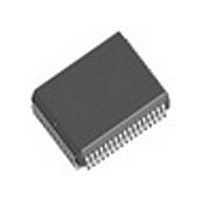
IC FIFO 1024X18 SYNC 25NS 68PLCC

IDT72245LB25J

Manufacturer Part Number
IDT72245LB25J
Description
IC FIFO 1024X18 SYNC 25NS 68PLCC
Manufacturer
IDT, Integrated Device Technology Inc
Series
7200r
Datasheet

Specifications of IDT72245LB25J

Function
Synchronous
Memory Size
18.4K (1K x 18)
Access Time
25ns
Voltage - Supply
4.5 V ~ 5.5 V
Operating Temperature
0°C ~ 70°C
Mounting Type
Surface Mount
Package / Case
68-PLCC
Configuration
Dual
Density
72Kb
Access Time (max)
15ns
Word Size
18b
Organization
4Kx18
Sync/async
Synchronous
Expandable
Yes
Bus Direction
Uni-Directional
Package Type
LCC
Clock Freq (max)
40MHz
Operating Supply Voltage (typ)
5V
Operating Supply Voltage (min)
4.5V
Operating Supply Voltage (max)
5.5V
Supply Current
60mA
Operating Temp Range
0C to 70C
Operating Temperature Classification
Commercial
Mounting
Surface Mount
Pin Count
68
Lead Free Status / RoHS Status
Contains lead / RoHS non-compliant
Data Rate
-
Lead Free Status / RoHS Status
Not Compliant, Contains lead / RoHS non-compliant
Other names
72245LB25J

Available stocks

Company
Part Number
Manufacturer
Quantity
Price
Part Number:
IDT72245LB25J
Manufacturer:
IDT
Quantity:
1 831
Part Number:
IDT72245LB25J
Manufacturer:
IDT, Integrated Device Technology Inc
Quantity:
10 000
Part Number:
IDT72245LB25J
Manufacturer:
IDT
Quantity:
253
Part Number:
IDT72245LB25J8
Manufacturer:
IDT, Integrated Device Technology Inc
Quantity:
10 000
Part Number:
IDT72245LB25J8
Manufacturer:
IDT
Quantity:
253
Part Number:
IDT72245LB25JB
Manufacturer:
IDT
Quantity:
238
FEATURES:
• • • • •
• • • • •
• • • • •
• • • • •
• • • • •
• • • • •
• • • • •
• • • • •
• • • • •
• • • • •
• • • • •
• • • • •
• • • • •
• • • • •
• • • • •
• • • • •
• • • • •
DESCRIPTION:
speed, low-power First-In, First-Out (FIFO) memories with clocked read and
FUNCTIONAL BLOCK DIAGRAM
IDT and the IDT logo are registered trademarks of Integrated Device Technology, Inc. SyncFIFO is a trademark of Integrated Device Technology, Inc.
COMMERCIAL AND INDUSTRIAL TEMPERATURE RANGES
©2008 Integrated Device Technology, Inc. All rights reserved. Product specifications subject to change without notice.
(
256 x 18-bit organization array (IDT72205LB)
512 x 18-bit organization array (IDT72215LB)
1,024 x 18-bit organization array (IDT72225LB)
2,048 x 18-bit organization array (IDT72235LB)
4,096 x 18-bit organization array (IDT72245LB)
10 ns read/write cycle time
Empy and Full flags signal FIFO status
Easy expandable in depth and width
Asynchronous or coincident read and write clocks
Programmable Almost-Empty and Almost-Full flags with
default settings
Half-Full flag capability
Dual-Port zero fall-through time architecture
Output enable puts output data bus in high-impedence state
High-performance submicron CMOS technology
Available in a 64-lead thin quad flatpack (TQFP/STQFP)
and plastic leaded chip carrier (PLCC)
Industrial temperature range (–40° ° ° ° ° C to +85° ° ° ° ° C) is available
Green parts available, see ordering information
The IDT72205LB/72215LB/72225LB/72235LB/72245LB are very high
)/
EXPANSION LOGIC
WRITE CONTROL
WRITE POINTER
RESET LOGIC
LOGIC
WCLK
CMOS SyncFIFO
256 x 18, 512 x 18, 1,024 x 18,
2,048 x 18, and 4,096 x 18
OUTPUT REGISTER
1,024 x 18, 2,048 x 18
256 x 18, 512 x 18
INPUT REGISTER
RAM ARRAY
4,096 x 18
TM
Q0-Q17
D0-D17
1
• •
• •
write controls. These FIFOs are applicable for a wide variety of data buffering
needs, such as optical disk controllers, Local Area Networks (LANs), and
interprocessor communication.
by a free-running clock (WCLK), and an input enable pin (WEN). Data is read
into the synchronous FIFO on every clock when WEN is asserted. The output
port is controlled by another clock pin (RCLK) and another enable pin (REN).
The read clock can be tied to the write clock for single clock operation or the
two clocks can run asynchronous of one another for dual-clock operation. An
Output Enable pin (OE) is provided on the read port for three-state control of
the output.
and two programmable flags, Almost-Empty (PAE) and Almost-Full (PAF). The
offset loading of the programmable flags is controlled by a simple state machine,
and is initiated by asserting the Load pin (LD). A Half-Full flag (HF) is available
when the FIFO is used in a single device configuration.
XI and XO pins are used to expand the FIFOs. In depth expansion configu-
ration, First Load (FL) is grounded on the first device and set to HIGH for all
other devices in the Daisy Chain.
using IDT’s high-speed submicron CMOS technology.
These FIFOs have 18-bit input and output ports. The input port is controlled
The synchronous FIFOs have two fixed flags, Empty (EF) and Full (FF),
These devices are depth expandable using a Daisy-Chain technique. The
The IDT72205LB/72215LB/72225LB/72235LB/72245LB is fabricated
OFFSET REGISTER
READ CONTROL
READ POINTER
RCLK
IDT72205LB, IDT72215LB,
IDT72225LB, IDT72235LB,
LOGIC
LOGIC
FLAG
OCTOBER 2008
IDT72245LB
2766 drw 01
/(
DSC-2766/2
)

Related parts for IDT72245LB25J

IDT72245LB25J Summary of contents

Page 1

FEATURES: • • • • • 256 x 18-bit organization array (IDT72205LB) • • • • • 512 x 18-bit organization array (IDT72215LB) • • • • • 1,024 x 18-bit organization array (IDT72225LB) • • • • • 2,048 ...

Page 2

IDT72205LB/72215LB/72225LB/72235LB/72245LB CMOS SyncFIFO 256 x 18, 512 x 18, 1,024 x 18, 2,048 x 18 and 4,096 x 18 PIN CONFIGURATIONS GND PIN ...

Page 3

IDT72205LB/72215LB/72225LB/72235LB/72245LB CMOS SyncFIFO 256 x 18, 512 x 18, 1,024 x 18, 2,048 x 18 and 4,096 x 18 PIN DESCRIPTION Symbol Name I/O D0–D17 Data Inputs I RS Reset I WCLK Write Clock I WEN Write Enable I RCLK ...

Page 4

IDT72205LB/72215LB/72225LB/72235LB/72245LB CMOS SyncFIFO 256 x 18, 512 x 18, 1,024 x 18, 2,048 x 18 and 4,096 x 18 ABSOLUTE MAXIMUM RATINGS Symbol Rating V Terminal Voltage TERM with respect to GND T Storage STG Temperature I DC Output Current ...

Page 5

IDT72205LB/72215LB/72225LB/72235LB/72245LB CMOS SyncFIFO 256 x 18, 512 x 18, 1,024 x 18, 2,048 x 18 and 4,096 ELECTRICAL CHARACTERISTICS (Commercial: VCC = 5V ± 10 0°C to +70°C; Industrial: VCC = 5V ± 10%, TA ...

Page 6

IDT72205LB/72215LB/72225LB/72235LB/72245LB CMOS SyncFIFO 256 x 18, 512 x 18, 1,024 x 18, 2,048 x 18 and 4,096 x 18 SIGNAL DESCRIPTIONS: INPUTS: DATA Data inputs for 18-bit wide data. CONTROLS: RESET (RS) Reset ...

Page 7

IDT72205LB/72215LB/72225LB/72235LB/72245LB CMOS SyncFIFO 256 x 18, 512 x 18, 1,024 x 18, 2,048 x 18 and 4,096 x 18 When the LD pin is LOW and WEN is HIGH, the WCLK input is disabled; then a signal at this input ...

Page 8

IDT72205LB/72215LB/72225LB/72235LB/72245LB CMOS SyncFIFO 256 x 18, 512 x 18, 1,024 x 18, 2,048 x 18 and 4,096 x 18 After half of the memory is filled, and at the LOW-to-HIGH transition of the next write cycle, the Half-Full Flag goes ...

Page 9

IDT72205LB/72215LB/72225LB/72235LB/72245LB CMOS SyncFIFO 256 x 18, 512 x 18, 1,024 x 18, 2,048 x 18 and 4,096 x 18 WCLK SKEW1 RCLK NOTE: is the minimum time between a rising RCLK edge and a ...

Page 10

IDT72205LB/72215LB/72225LB/72235LB/72245LB CMOS SyncFIFO 256 x 18, 512 x 18, 1,024 x 18, 2,048 x 18 and 4,096 x 18 WCLK (first valid write ENS RCLK ...

Page 11

IDT72205LB/72215LB/72225LB/72235LB/72245LB CMOS SyncFIFO 256 x 18, 512 x 18, 1,024 x 18, 2,048 x 18 and 4,096 x 18 WCLK t DS DATA WRITE ENS t ENH t t SKEW2 RCLK LOW Q ...

Page 12

IDT72205LB/72215LB/72225LB/72235LB/72245LB CMOS SyncFIFO 256 x 18, 512 x 18, 1,024 x 18, 2,048 x 18 and 4,096 x 18 WCLK RCLK NOTE PAE offset. Number of data words written into FIFO already = n. WCLK D – ...

Page 13

IDT72205LB/72215LB/72225LB/72235LB/72245LB CMOS SyncFIFO 256 x 18, 512 x 18, 1,024 x 18, 2,048 x 18 and 4,096 x 18 WCLK t ENS NOTE: 1. Write to Last Physical Location. RCLK t ENS NOTE: 1. Read from Last Physical Location. WCLK ...

Page 14

IDT72205LB/72215LB/72225LB/72235LB/72245LB CMOS SyncFIFO 256 x 18, 512 x 18, 1,024 x 18, 2,048 x 18 and 4,096 x 18 OPERATING CONFIGURATIONS SINGLE DEVICE CONFIGURATION A single IDT72205LB/72215LB/72225LB/72235LB/72245LB may be used when the application requirements are for 256/512/1,024/2,048/4,096 words WRITE CLOCK ...

Page 15

IDT72205LB/72215LB/72225LB/72235LB/72245LB CMOS SyncFIFO 256 x 18, 512 x 18, 1,024 x 18, 2,048 x 18 and 4,096 x 18 DEPTH EXPANSION CONFIGURATION — (WITH PROGRAMMABLE FLAGS) These devices can easily be adapted to applications requiring more than 256/ 512/1,024/2,048/4,096 words ...

Page 16

ORDERING INFORMATION XXXXX X XX Device Type Power Speed Package NOTES: 1. Industrial temperature range product for 15ns and 25ns speed grades are available as a standard device. All other speed grades are available by special order. 2. Green parts ...

Related keywords