IDT72V265LA15TFI IDT, Integrated Device Technology Inc, IDT72V265LA15TFI Datasheet - Page 2
IDT72V265LA15TFI
Manufacturer Part Number
IDT72V265LA15TFI
Description
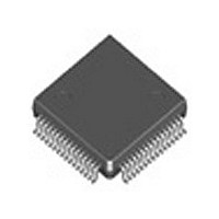
IC FIFO SS 16384X18 15NS 64STQFP
Manufacturer
IDT, Integrated Device Technology Inc
Series
72Vr
Datasheet
1.IDT72V255LA10TFG.pdf
(27 pages)
Specifications of IDT72V265LA15TFI
Function
Synchronous
Memory Size
288K (16K x 18)
Data Rate
67MHz
Access Time
15ns
Voltage - Supply
3 V ~ 3.6 V
Operating Temperature
-40°C ~ 85°C
Mounting Type
Surface Mount
Package / Case
64-STQFP
Configuration
Dual
Density
288Kb
Access Time (max)
10ns
Word Size
18b
Organization
16Kx18
Sync/async
Synchronous
Expandable
Yes
Bus Direction
Uni-Directional
Package Type
STQFP
Clock Freq (max)
66.7MHz
Operating Supply Voltage (typ)
3.3V
Operating Supply Voltage (min)
3V
Operating Supply Voltage (max)
3.6V
Supply Current
55mA
Operating Temp Range
-40C to 85C
Operating Temperature Classification
Industrial
Mounting
Surface Mount
Pin Count
64
Lead Free Status / RoHS Status
Contains lead / RoHS non-compliant
Other names
72V265LA15TFI
Available stocks
Company
Part Number
Manufacturer
Quantity
Price
Company:

Part Number:
IDT72V265LA15TFI
Manufacturer:
IDT, Integrated Device Technology Inc
Quantity:
10 000
Company:
Part Number:
IDT72V265LA15TFI8
Manufacturer:
IDT, Integrated Device Technology Inc
Quantity:
10 000


DESCRIPTION (CONTINUED)
PIN CONFIGURATIONS
NOTE:
1. DC = Don’t Care. Must be tied to GND or V
• • • • •
• • • • •
telecommunications, data communications and other applications that need to
buffer large amounts of data.
IDT72V255LA/72V265LA 3.3 VOLT CMOS SuperSync FIFO™
8,192 x 18, 16,384 x 18
The period required by the retransmit operation is now fixed and short.
The first word data latency period, from the time the first word is written to
an empty FIFO to the time it can be read, is now fixed and short. (The variable
clock cycle counting delay associated with the latency period found on
previous SuperSync devices has been eliminated on this SuperSync
family.)
SuperSync FIFOs are particularly appropriate for networking, video,
PIN 1
DC
WEN
GND
SEN
D17
D16
D15
D14
D13
D12
D11
D10
V
D9
D8
D7
CC
(1)
CC
, cannot be left open.
1
2
3
4
5
6
7
8
9
10
11
12
13
14
15
16
64 63 62 61 60 59 58 57 56 55 54 53 52 51 50 49
17 18 19 20 21 22 23 24 25 26 27 28 29 30 31 32
STQFP (PP64-1, ORDER CODE: TF)
TQFP (PN64-1, ORDER CODE: PF)
TOP VIEW
2
(WEN) input. Data is written into the FIFO on every rising edge of WCLK when
WEN is asserted. The output port is controlled by a Read Clock (RCLK) input
and Read Enable (REN) input. Data is read from the FIFO on every rising
edge of RCLK when REN is asserted. An Output Enable (OE) input is provided
for three-state control of the outputs.
to fMAX with complete independence. There are no restrictions on the
frequency of one clock input with respect to the other.
The input port is controlled by a Write Clock (WCLK) input and a Write Enable
The frequencies of both the RCLK and the WCLK signals may vary from 0
48
47
46
45
44
43
42
41
40
39
38
37
36
35
34
33
COMMERCIAL AND INDUSTRIAL
4672 drw 02
TEMPERATURE RANGES
Q17
Q16
GND
Q15
Q14
V
Q13
Q12
Q11
GND
Q10
Q9
Q8
Q7
Q6
GND
CC
OCTOBER 22, 2008
Related parts for IDT72V265LA15TFI
Image
Part Number
Description
Manufacturer
Datasheet
Request
R

Part Number:
Description:
TRANSLATION DEVICE DPI 80-PQFP
Manufacturer:
IDT, Integrated Device Technology Inc
Datasheet:
Part Number:
Description:
IDT PART
Manufacturer:
IDT, Integrated Device Technology Inc
Datasheet:
Part Number:
Description:
IC LIU T1/E1/J1 OCTAL 256PBGA
Manufacturer:
IDT, Integrated Device Technology Inc
Datasheet:

Part Number:
Description:
IC FREQ TIMING GENERATOR 28TSSOP
Manufacturer:
IDT, Integrated Device Technology Inc
Datasheet:
Part Number:
Description:
IC CLK DVR PLL 1:10 40VFQFPN
Manufacturer:
IDT, Integrated Device Technology Inc
Datasheet:
Part Number:
Description:
IC CLK FANOUT BUFFER 1:18 32LQFP
Manufacturer:
IDT, Integrated Device Technology Inc
Datasheet:
Part Number:
Description:
IC CLK FANOUT BUFFER 1:18 32LQFP
Manufacturer:
IDT, Integrated Device Technology Inc
Datasheet:
Part Number:
Description:
IC CK505 VREG/RES 56TSSOP
Manufacturer:
IDT, Integrated Device Technology Inc
Datasheet:

Part Number:
Description:
IC SDRAM CLK DVR 1:10 48-TSSOP
Manufacturer:
IDT, Integrated Device Technology Inc
Datasheet:

Part Number:
Description:
IC CLK DVR PLL 1:10 48TSSOP
Manufacturer:
IDT, Integrated Device Technology Inc
Datasheet:
Part Number:
Description:
IC FLEXPC CLK PROGR P4 56-TSSOP
Manufacturer:
IDT, Integrated Device Technology Inc
Datasheet:
Part Number:
Description:
IC FLEXPC CLK PROGR P4 56-TSSOP
Manufacturer:
IDT, Integrated Device Technology Inc
Datasheet:
Part Number:
Description:
IC FLEXPC CLK PROGR P4 56-SSOP
Manufacturer:
IDT, Integrated Device Technology Inc
Datasheet:

Part Number:
Description:
IC PLL CLK DRIVER 2.5V 28-TSSOP
Manufacturer:
IDT, Integrated Device Technology Inc
Datasheet:
Part Number:
Description:
IC CLOCK DRIVER 2.5V 24-TSSOP
Manufacturer:
IDT, Integrated Device Technology Inc
Datasheet: