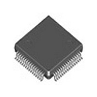
IDT72V265LA15TFI IDT, Integrated Device Technology Inc, IDT72V265LA15TFI Datasheet - Page 6

IDT72V265LA15TFI
Manufacturer Part Number
IDT72V265LA15TFI
Description
IC FIFO SS 16384X18 15NS 64STQFP
Manufacturer
IDT, Integrated Device Technology Inc
Series
72Vr
Datasheet
1.IDT72V255LA10TFG.pdf
(27 pages)
Specifications of IDT72V265LA15TFI
Function
Synchronous
Memory Size
288K (16K x 18)
Data Rate
67MHz
Access Time
15ns
Voltage - Supply
3 V ~ 3.6 V
Operating Temperature
-40°C ~ 85°C
Mounting Type
Surface Mount
Package / Case
64-STQFP
Configuration
Dual
Density
288Kb
Access Time (max)
10ns
Word Size
18b
Organization
16Kx18
Sync/async
Synchronous
Expandable
Yes
Bus Direction
Uni-Directional
Package Type
STQFP
Clock Freq (max)
66.7MHz
Operating Supply Voltage (typ)
3.3V
Operating Supply Voltage (min)
3V
Operating Supply Voltage (max)
3.6V
Supply Current
55mA
Operating Temp Range
-40C to 85C
Operating Temperature Classification
Industrial
Mounting
Surface Mount
Pin Count
64
Lead Free Status / RoHS Status
Contains lead / RoHS non-compliant
Other names
72V265LA15TFI
Available stocks
Company
Part Number
Manufacturer
Quantity
Price
Company:
Part Number:
IDT72V265LA15TFI
Manufacturer:
IDT, Integrated Device Technology Inc
Quantity:
10 000
Company:
Part Number:
IDT72V265LA15TFI8
Manufacturer:
IDT, Integrated Device Technology Inc
Quantity:
10 000
AC ELECTRICAL CHARACTERISTICS
(Commercial: V
AC TEST CONDITIONS
IDT72V255LA/72V265LA 3.3 VOLT CMOS SuperSync FIFO™
8,192 x 18, 16,384 x 18
NOTES:
1. All AC timings apply to both Standard IDT mode and First Word Fall Through mode.
2. Industrial temperature range product for 15ns speed grade is available as a standard device.
3. Pulse widths less than minimum values are not allowed.
4. Values guaranteed by design, not currently tested.
Symbol
f
t
t
t
t
t
t
t
t
t
t
t
t
t
t
t
t
t
t
t
t
t
t
t
t
t
t
t
t
S
A
CLK
DH
ENH
LDS
LDH
RSR
CLKH
CLKL
DS
ENS
RS
RSS
RSF
FWFT
RTS
OLZ
OE
OHZ
WFF
REF
PAF
PAE
HF
SKEW1
SKEW2
SKEW3
SKEW4
Input Pulse Levels
Input Rise/Fall Times
Input Timing Reference Levels
Output Reference Levels
Output Load
Clock Cycle Frequency
Data Access Time
Clock Cycle Time
Clock High Time
Clock Low Time
Data Setup Time
Data Hold Time
Enable Setup Time
Enable Hold Time
Load Setup Time
Load Hold Time
Reset Pulse Width
Reset Setup Time
Reset Recovery Time
Reset to Flag and Output Time
Mode Select Time
Retransmit Setup Time
Output Enable to Output in Low Z
Output Enable to Output Valid
Output Enable to Output in High Z
Write Clock to FF or IR
Read Clock to EF or OR
Write Clock to PAF
Read Clock to PAE
Clock to HF
Skew time between RCLK and WCLK for FF/IR
Skew time between RCLK and WCLK for PAE and PAF
Skew time between RCLK and WCLK for EF/OR
Skew time between RCLK and WCLK for PAE and PAF
for Re-transmit operation
CC
= 3.3V ± 0.3V, T
(3)
Parameter
A
= 0°C to +70°C; Industrial: V
(4)
(4)
GND to 3.0V
See Figure 2
1.5V
1.5V
3ns
CC
3.3V ± 0.3V,T
Min.
4.5
4.5
0.5
0.5
0.5
10
10
10
10
12
60
15
—
—
—
—
—
—
—
2
3
3
3
0
3
0
2
2
5
IDT72V255LA10
IDT72V265LA10
Commercial
(1)
6
* Includes jig and scope capacitances.
Max.
100
6.5
6.5
6.5
6.5
6.5
A
—
—
—
—
—
—
—
—
—
—
—
—
10
—
—
—
16
—
—
—
—
6
6
= -40°C to +85°C)
D.U.T.
Min.
IDT72V255LA15
IDT72V265LA15
Com’l & Ind’l
15
15
15
15
15
60
17
—
—
—
—
—
—
—
2
6
6
4
1
4
1
4
1
0
4
0
3
3
6
510Ω
Figure 2. Output Load
66.7
Max.
10
15
10
10
10
10
20
—
—
—
—
—
—
—
—
—
—
—
—
—
—
—
—
—
—
—
(2)
8
8
3.3V
COMMERCIAL AND INDUSTRIAL
330Ω
30pF*
Min.
IDT72V255LA20
IDT72V265LA20
20
20
20
20
—
10
20
60
25
—
—
—
—
—
—
2
8
8
5
1
5
1
5
1
0
5
0
3
3
TEMPERATURE RANGES
Commercial
OCTOBER 22, 2008
4672 drw 04
Max.
50
12
20
10
10
12
12
12
12
22
—
—
—
—
—
—
—
—
—
—
—
—
—
—
—
—
—
—
—
Unit
M H z
ns
ns
ns
ns
ns
ns
ns
ns
ns
ns
ns
ns
ns
ns
ns
ns
ns
ns
ns
ns
ns
ns
ns
ns
ns
ns
ns
ns


