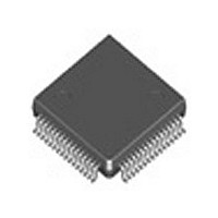
IDT72V265LA15TFI IDT, Integrated Device Technology Inc, IDT72V265LA15TFI Datasheet - Page 4

IDT72V265LA15TFI
Manufacturer Part Number
IDT72V265LA15TFI
Description
IC FIFO SS 16384X18 15NS 64STQFP
Manufacturer
IDT, Integrated Device Technology Inc
Series
72Vr
Datasheet
1.IDT72V255LA10TFG.pdf
(27 pages)
Specifications of IDT72V265LA15TFI
Function
Synchronous
Memory Size
288K (16K x 18)
Data Rate
67MHz
Access Time
15ns
Voltage - Supply
3 V ~ 3.6 V
Operating Temperature
-40°C ~ 85°C
Mounting Type
Surface Mount
Package / Case
64-STQFP
Configuration
Dual
Density
288Kb
Access Time (max)
10ns
Word Size
18b
Organization
16Kx18
Sync/async
Synchronous
Expandable
Yes
Bus Direction
Uni-Directional
Package Type
STQFP
Clock Freq (max)
66.7MHz
Operating Supply Voltage (typ)
3.3V
Operating Supply Voltage (min)
3V
Operating Supply Voltage (max)
3.6V
Supply Current
55mA
Operating Temp Range
-40C to 85C
Operating Temperature Classification
Industrial
Mounting
Surface Mount
Pin Count
64
Lead Free Status / RoHS Status
Contains lead / RoHS non-compliant
Other names
72V265LA15TFI
Available stocks
Company
Part Number
Manufacturer
Quantity
Price
Company:
Part Number:
IDT72V265LA15TFI
Manufacturer:
IDT, Integrated Device Technology Inc
Quantity:
10 000
Company:
Part Number:
IDT72V265LA15TFI8
Manufacturer:
IDT, Integrated Device Technology Inc
Quantity:
10 000
PIN DESCRIPTION
IDT72V255LA/72V265LA 3.3 VOLT CMOS SuperSync FIFO™
8,192 x 18, 16,384 x 18
Symbol
D
MRS
PRS
RT
FWFT/SI
WCLK
WEN
RCLK
REN
OE
SEN
LD
DC
FF/IR
EF/OR
PAF
PAE
Q
V
GND
HF
0
CC
0
–D
–Q
17
17
Name
Data Inputs
Master Reset
Partial Reset
Retransmit
First Word Fall
Through/Serial In
Write Clock
Write Enable
Read Clock
Read Enable
Output Enable
Serial Enable
Load
Don't Care
Full Flag/
Empty Flag/
Output Ready
Programmable
Almost-Full Flag
Programmable
Almost-Empty Flag
Half-Full Flag
Data Outputs
Power
Ground
Input Ready
I/O
O
O
O
O
O
O
I
I
I
I
I
I
I
I
I
I
I
I
I
Data inputs for a 18-bit bus.
MRS initializes the read and write pointers to zero and sets the output register to all zeroes. During
Master Reset, the FIFO is configured for either FWFT or IDT Standard mode, one of two program
mable flag default settings, and serial or parallel programming of the offset settings.
PRS initializes the read and write pointers to zero and sets the output register to all zeroes. During
Partial Reset, the existing mode (IDT or FWFT), programming method (serial or parallel), and
programmable flag settings are all retained.
RT asserted on the rising edge of RCLK initializes the READ pointer to zero, sets the EF flag to
LOW (OR to HIGH in FWFT mode) temporarily and does not disturb the write pointer, programming
method, existing timing mode or programmable flag settings. RT is useful to reread data from the first
physical location of the FIFO.
During Master Reset, selects First Word Fall Through or IDT Standard mode. After Master Reset,
this pin functions as a serial input for loading offset registers
When enabled by WEN, the rising edge of WCLK writes data into the FIFO and offsets into the
programmable registers for parallel programming, and when enabled by SEN, the rising edge of
WCLK writes one bit of data into the programmable register for serial programming.
WEN enables WCLK for writing data into the FIFO memory and offset registers.
REN enables RCLK for reading data from the FIFO memory and offset registers.
OE controls the output impedance of Q
SEN enables serial loading of programmable flag offsets.
During Master Reset, LD selects one of two partial flag default offsets (127 or 1,023) and determines
the flag offset programming method, serial or parallel. After Master Reset, this pin enables writing to
and reading from the offset registers.
This pin must be tied to either V
In the IDT Standard mode, the FF function is selected. FF indicates whether or not the FIFO
memory is full. In the FWFT mode, the IR function is selected. IR indicates whether or not
there is space available for writing to the FIFO memory.
In the IDT Standard mode, the EF function is selected. EF indicates whether or not the FIFO
memory is empty. In FWFT mode, the OR function is selected. OR indicates whether or not there is
valid data available at the outputs.
PAF goes LOW if the number of words in the FIFO memory is more than total word capacity of the
FIFO minus the full offset value m, which is stored in the Full Offset register. There are two possible
default values for m: 127 or 1,023.
PAE goes LOW if the number of words in the FIFO memory is less than offset n, which is stored in
the Empty Offset register. There are two possible default values for n: 127 or 1,023. Other values
for n can be programmed into the device.
HF indicates whether the FIFO memory is more or less than half-full.
Data outputs for an 18-bit bus.
+3.3 Volt power supply pins.
Ground pins.
When enabled by REN, the rising edge of RCLK reads data from the FIFO memory and offsetsfrom
the programmable registers.
4
CC
or GND and must not toggle after Master Reset.
Description
n.
COMMERCIAL AND INDUSTRIAL
TEMPERATURE RANGES
OCTOBER 22, 2008


