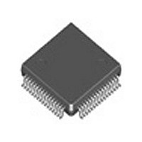
IDT72V265LA15TFI IDT, Integrated Device Technology Inc, IDT72V265LA15TFI Datasheet - Page 9

IDT72V265LA15TFI
Manufacturer Part Number
IDT72V265LA15TFI
Description
IC FIFO SS 16384X18 15NS 64STQFP
Manufacturer
IDT, Integrated Device Technology Inc
Series
72Vr
Datasheet
1.IDT72V255LA10TFG.pdf
(27 pages)
Specifications of IDT72V265LA15TFI
Function
Synchronous
Memory Size
288K (16K x 18)
Data Rate
67MHz
Access Time
15ns
Voltage - Supply
3 V ~ 3.6 V
Operating Temperature
-40°C ~ 85°C
Mounting Type
Surface Mount
Package / Case
64-STQFP
Configuration
Dual
Density
288Kb
Access Time (max)
10ns
Word Size
18b
Organization
16Kx18
Sync/async
Synchronous
Expandable
Yes
Bus Direction
Uni-Directional
Package Type
STQFP
Clock Freq (max)
66.7MHz
Operating Supply Voltage (typ)
3.3V
Operating Supply Voltage (min)
3V
Operating Supply Voltage (max)
3.6V
Supply Current
55mA
Operating Temp Range
-40C to 85C
Operating Temperature Classification
Industrial
Mounting
Surface Mount
Pin Count
64
Lead Free Status / RoHS Status
Contains lead / RoHS non-compliant
Other names
72V265LA15TFI
Available stocks
Company
Part Number
Manufacturer
Quantity
Price
Company:
Part Number:
IDT72V265LA15TFI
Manufacturer:
IDT, Integrated Device Technology Inc
Quantity:
10 000
Company:
Part Number:
IDT72V265LA15TFI8
Manufacturer:
IDT, Integrated Device Technology Inc
Quantity:
10 000
IDT72V255LA/72V265LA 3.3 VOLT CMOS SuperSync FIFO™
8,192 x 18, 16,384 x 18
17
17
NOTES:
1. The programming method can only be selected at Master Reset.
2. Parallel reading of the offset registers is always permitted regardless of which programming method has been selected.
3. The programming sequence applies to both IDT Standard and FWFT modes.
LD
0
0
0
X
1
1
1
IDT72V255LA ⎯ 8,192 x 18 - BIT
12
12
3FFH if LD is HIGH at Master Reset
3FFH if LD is HIGH at Master Reset
07FH if LD is LOW at Master Reset,
07FH if LD is LOW at Master Reset,
WEN
EMPTY OFFSET REGISTER
X
FULL OFFSET REGISTER
0
1
1
1
0
1
DEFAULT VALUE
DEFAULT VALUE
REN
X
1
0
1
1
0
1
Figure 4. Programmable Flag Offset Programming Sequence
Figure 3. Offset Register Location and Default Values
SEN
X
1
1
0
1
X
X
WCLK
X
X
X
X
0
0
9
17
17
RCLK
X
X
X
X
X
IDT72V265LA ⎯ 16,384 x 18 - BIT
13
13
Parallel write to registers:
Empty Offset
Full Offset
Parallel read from registers:
Serial shift into registers:
26 bits for the 72V255LA
28 bits for the 72V265LA
1 bit for each rising WCLK edge
Starting with Empty Offset (LSB)
Ending with Full Offset (MSB)
No Operation
Write Memory
Read Memory
No Operation
Empty Offset
Full Offset
3FFH if LD is HIGH at Master Reset
3FFH if LD is HIGH at Master Reset
07FH if LD is LOW at Master Reset,
07FH if LD is LOW at Master Reset,
EMPTY OFFSET REGISTER
FULL OFFSET REGISTER
DEFAULT VALUE
DEFAULT VALUE
COMMERCIAL AND INDUSTRIAL
Selection
TEMPERATURE RANGES
OCTOBER 22, 2008
4672 drw 07
4672 drw 06
0
0


