FXL2TD245L10X Fairchild Semiconductor, FXL2TD245L10X Datasheet
FXL2TD245L10X
Specifications of FXL2TD245L10X
Available stocks


Related parts for FXL2TD245L10X


FXL2TD245L10X Summary of contents
Page 1
... Ports by placing them in a 3-STATE condition. The FXL2TD245 is designed so that the control pins (T/R and OE) are supplied CCA Ordering Information Order Number Package Number FXL2TD245L10X Pb-Free package per JEDEC J-STD-020B. ©2005 Fairchild Semiconductor Corporation FXL2TD245 Rev. 1.0.4 Features ■ Bi-directional interface between any 2 levels from 1.1V to 3.6V ■ ...
Page 2
... A 1 T/R 1 Connection Diagram CCB CCA 0 1 (Top View) Pin Assignment Pin Number Terminal Name ©2005 Fairchild Semiconductor Corporation FXL2TD245 Rev. 1.0.4 Pin Descriptions Pin Names V CCB OE T CCA 0 V CCB Truth Table Inputs HIGH Voltage Level T LOW Voltage Level ...
Page 3
... T Free Air Operating Temperature A ∆t /∆V Maximum Input Edge Rate V Notes Absolute Maximum Rating must be observed All unused inputs and input/output pins must be held at V ©2005 Fairchild Semiconductor Corporation FXL2TD245 Rev. 1.0.4 Parameter , OE < (2) ...
Page 4
... OL (4) Voltage Input Leakage V I Current Control Pins ©2005 Fairchild Semiconductor Corporation FXL2TD245 Rev. 1.0.4 V (V) Conditions CCI , B 2.7–3 2.3–2.7 1.65–2.3 1.4–1.65 1.1–1.4 2.7–3 CCA 2.3–2.7 1.65–2.3 1.4–1.65 1.1–1 2.7–3 2.3– ...
Page 5
... V associated with the data input under test. CCI CC = the associated with the output under test. CCO CC 5. Don't Care = Any valid logic level. 6. Reflects current per supply, V CCA ©2005 Fairchild Semiconductor Corporation FXL2TD245 Rev. 1.0.4 (Continued) V (V) Conditions CCI = ...
Page 6
... Parameter Propagation Delay PLH PHL Propagation Delay Output Enable PZH PZL Output Enable Output Disable PHZ PLZ Output Disable ©2005 Fairchild Semiconductor Corporation FXL2TD245 Rev. 1.0.4 = -40°C to +85° CCB = = V V 1.65V to CCB CCB 3.0V to 3.6V 2.3V to 2.7V 1.95V Min. Max. ...
Page 7
... Output Disable PHZ PLZ Output Disable Capacitance Symbol Parameter C Input Capacitance Control Pins (OE, T/Rn Input/Output Capacitance A I/O C Power Dissipation Capacitance PD ©2005 Fairchild Semiconductor Corporation FXL2TD245 Rev. 1.0.4 (Continued) = -40°C to +85° CCB = = V V 1.65V to CCB CCB 3.0V to 3.6V 2.3V to 2.7V 1 ...
Page 8
... CCI CCO 0. 0. For for Control Pins T/R and OE CCI CCA ©2005 Fairchild Semiconductor Corporation FXL2TD245 Rev. 1.0 Rtr1 DUT Test Switch , t OPEN PLH PHL = 3.3 ± 0.3V, 2.5V ± 0.2V CCO CCO , t PLZ PZL 1.8V ± 0.15V, 1.5V ± 0.1V, 1.2V ± 0.1V ...
Page 9
... Tape and Reel Specification Tape Format for MicroPak 10 Package Designator Section L10X Leader (Start End) Trailer (Hub End) Tape Dimensions inches (millimeters) ©2005 Fairchild Semiconductor Corporation FXL2TD245 Rev. 1.0.4 Tape Number Cavities 125 (typ) Carrier 5000 75 (typ) 9 Cavity Cover Tape Status ...
Page 10
... MicroPak 10 Reel Dimensions Tape Size 7.0 0.059 0.512 (177.8) (1.50) (13.00) ©2005 Fairchild Semiconductor Corporation FXL2TD245 Rev. 1.0.4 inches (millimeters 0.331 + 0.059/-0.000 0.795 2.165 (8.40 + 1.50/-0.00) (20.20) (55.00 0.078/-0.039W 0.567 (W1 + 2.00/-1.00) (14.40) www.fairchildsemi.com ...
Page 11
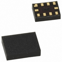
... Physical Dimensions inches (millimeters) unless otherwise noted ©2005 Fairchild Semiconductor Corporation FXL2TD245 Rev. 1.0.4 Pb-Free 10-Lead MicroPak, 1.6mm x 2.1mm Package Number MAC010A 11 www.fairchildsemi.com ...
Page 12
... FAIRCHILD SEMICONDUCTOR TRADEMARKS The following are registered and unregistered trademarks Fairchild Semiconductor owns or is authorized to use and is not intended exhaustive list of all such trademarks. ACEx™ FACT Quiet Series™ ActiveArray™ GlobalOptoisolator™ Bottomless™ GTO™ Build it Now™ ...