FXL2TD245L10X Fairchild Semiconductor, FXL2TD245L10X Datasheet - Page 2
FXL2TD245L10X
Manufacturer Part Number
FXL2TD245L10X
Description
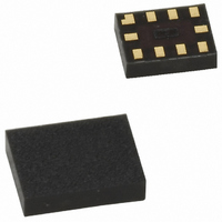
TRANSLATOR 2BIT LV DL 10MICROPAK
Manufacturer
Fairchild Semiconductor
Datasheet
1.FXL2TD245L10X.pdf
(12 pages)
Specifications of FXL2TD245L10X
Logic Function
Translator, 3-State
Number Of Bits
2
Input Type
Voltage
Output Type
Voltage
Number Of Channels
1
Number Of Outputs/channel
2
Differential - Input:output
No/No
Propagation Delay (max)
3.5ns
Voltage - Supply
1.1 V ~ 3.6 V
Operating Temperature
-40°C ~ 85°C
Package / Case
10-MicroPak™
Supply Voltage
1.1 V ~ 3.6 V
Logic Type
CMOS
Logic Family
FXL
Number Of Channels Per Chip
2
High Level Output Current
- 24 mA
Low Level Output Current
24 mA
Propagation Delay Time
24 ns
Supply Voltage (max)
3.6 V
Supply Voltage (min)
1.1 V
Maximum Operating Temperature
+ 85 C
Function
Bus Transceiver
Input Bias Current (max)
20 uA
Minimum Operating Temperature
- 40 C
Mounting Style
SMD/SMT
Number Of Circuits
1
Polarity
Non-Inverting
Operating Supply Voltage (typ)
1.8/2.5/3.3V
Number Of Elements
1
Package Type
MicroPak W
Logical Function
Bus Transceiver
Operating Supply Voltage (min)
1.1V
Operating Supply Voltage (max)
3.6V
Technology
CMOS
Operating Temp Range
-40C to 85C
Operating Temperature Classification
Industrial
Mounting
Surface Mount
Pin Count
10
Lead Free Status / RoHS Status
Lead free / RoHS Compliant
Data Rate
-
Lead Free Status / Rohs Status
Lead free / RoHS Compliant
Other names
FXL2TD245L10XTR
Available stocks
Company
Part Number
Manufacturer
Quantity
Price

Part Number:
FXL2TD245L10X
Manufacturer:
FAIRCHILD/仙童
Quantity:
20 000


©2005 Fairchild Semiconductor Corporation
FXL2TD245 Rev. 1.0.4
Functional Diagram
Connection Diagram
Pin Assignment
T/R
T/R
OE
A
A
0
0
1
1
Pin Number
V
CCB
10
1
2
3
4
5
6
7
8
9
V
B
10
CCA
1
9
V
0
CCA
(Top View)
B
A
8
2
1
0
OE
A
7
3
1
Terminal Name
T/R
T/R
6
5
4
V
V
GND
T/R
T/R
OE
CCA
A
A
B
B
CCB
V
1
0
0
1
1
0
CCB
GND
0
1
B
B
0
1
2
Pin Descriptions
Truth Table
H = HIGH Voltage Level
L = LOW Voltage Level
X = Don't Care
Power-Up/Power-Down Sequencing
FXL translators offer an advantage in that either V
may be powered up first. This benefit derives from the
chip design. When either V
a HIGH-Impedance state. The control inputs (T/R
OE) are designed to track the V
resistor tying OE to V
bus contention, excessive currents, or oscillations do not
occur during power-up/power-down. The size of the pull-
up resistor is based upon the current-sinking capability
of the OE driver.
The recommended power-up sequence is the following:
1. Apply power to either V
2. Apply power to the T/R
3. Apply power to other V
4. Drive the OE input LOW to enable the device.
The recommended power-down sequence is the follow-
ing:
1. Drive OE input HIGH to disable the device.
2. Remove power from either V
3. Remove power from other V
Pin Names
OE T/R
H
L
L
L
L
operation; Logic LOW for B-to-A operation) and to the
respective data inputs (A Port or B Port). This may
occur at the same time as Step 1.
V
V
T/R
OE
Inputs
A
B
CCA
CCB
n
n
n
H
X
X
X
L
0
T/R
H
X
X
X
L
Output Enable Input
Transmit/Receive Inputs
Side A Inputs or 3-STATE Outputs
Side B Inputs or 3-STATE Outputs
Side A Power Supply
Side B Power Supply
1
B
A
B
A
3-STATE
CCA
0
0
1
1
Data to A
Data to B
Data to A
Data to B
n
CC
should be used to ensure that
CC
CC
inputs (Logic HIGH for A-to-B
.
.
Description
is at 0 volts, outputs are in
CC
CC
0
0
1
1
Outputs
.
CCA
.
Output
Output
Output
Output
supply. A pull-up
www.fairchildsemi.com
n
and
CC
Related parts for FXL2TD245L10X
Image
Part Number
Description
Manufacturer
Datasheet
Request
R

Part Number:
Description:
Fairchild Semiconductor [IGBT MODULE]
Manufacturer:
Fairchild Semiconductor
Datasheet:

Part Number:
Description:
Discrete Semiconductor Modules
Manufacturer:
Fairchild Semiconductor
Part Number:
Description:
Discrete Semiconductor Modules
Manufacturer:
Fairchild Semiconductor
Part Number:
Description:
This N-Channel MOSFET is produced using Fairchild Semiconductor’s advanced Power Trench® process
Manufacturer:
Fairchild Semiconductor
Datasheet:
Part Number:
Description:
This N-Channel MOSFET is produced using Fairchild Semiconductor’s advanced Power Trench® process
Manufacturer:
Fairchild Semiconductor
Datasheet:
Part Number:
Description:
This N-Channel MOSFET is produced using Fairchild Semiconductor’s advanced PowerTrench® process
Manufacturer:
Fairchild Semiconductor
Datasheet:
Part Number:
Description:
This N-Channel MOSFET is produced using Fairchild Semiconductor’s advanced PowerTrench® process
Manufacturer:
Fairchild Semiconductor
Datasheet:
Part Number:
Description:
This N-Channel MOSFET is produced using Fairchild Semiconductor’s advanced Power Trench® process
Manufacturer:
Fairchild Semiconductor
Datasheet:
Part Number:
Description:
This N-Channel logic Level MOSFETs are produced using Fairchild Semiconductor‘s advanced Power Trench® process that has been special tailored to minimize the on-state resistance and yet maintain superior switching performance
Manufacturer:
Fairchild Semiconductor
Datasheet:
Part Number:
Description:
This N-Channel MOSFET is produced using Fairchild Semiconductor’s advanced Power Trench® process
Manufacturer:
Fairchild Semiconductor
Datasheet:
Part Number:
Description:
This N-Channel SyncFET™ is produced using Fairchild Semiconductor’s advanced PowerTrench® process
Manufacturer:
Fairchild Semiconductor
Datasheet:
Part Number:
Description:
This N-Channel SyncFET™ is produced using Fairchild Semiconductor’s advanced PowerTrench® process
Manufacturer:
Fairchild Semiconductor
Datasheet:
Part Number:
Description:
This N-Channel SyncFET™ is produced using Fairchild Semiconductor’s advanced PowerTrench® process
Manufacturer:
Fairchild Semiconductor
Datasheet:
Part Number:
Description:
This N-Channel logic Level MOSFETs are produced using Fairchild Semiconductor‘s advanced Power Trench® process that has been special tailored to minimize the on-state resistance and yet maintain superior switching performance
Manufacturer:
Fairchild Semiconductor
Datasheet:
Part Number:
Description:
This N-Channel MOSFET is produced using Fairchild Semiconductor’s advanced Power Trench® process that has been especially tailored to minimize the on-state resistance and yet maintain superior switching performance
Manufacturer:
Fairchild Semiconductor
Datasheet: