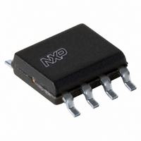
PCF85102C-2T/03,11 NXP Semiconductors, PCF85102C-2T/03,11 Datasheet - Page 17

PCF85102C-2T/03,11
Manufacturer Part Number
PCF85102C-2T/03,11
Description
IC EEPROM 2KBIT 100KHZ 8SOIC
Manufacturer
NXP Semiconductors
Datasheet
1.PCF85102C-2T0311.pdf
(20 pages)
Specifications of PCF85102C-2T/03,11
Memory Size
2K (256 x 8)
Package / Case
8-SOIC (3.9mm Width)
Format - Memory
EEPROMs - Serial
Memory Type
EEPROM
Speed
100kHz
Interface
I²C, 2-Wire Serial
Voltage - Supply
2.5 V ~ 6.0 V
Operating Temperature
-40°C ~ 85°C
Organization
256 K x 8
Interface Type
I2C
Maximum Clock Frequency
0.1 MHz
Supply Voltage (max)
6 V
Supply Voltage (min)
2.5 V
Maximum Operating Current
2 mA
Maximum Operating Temperature
+ 85 C
Mounting Style
SMD/SMT
Minimum Operating Temperature
- 40 C
Operating Supply Voltage
3.3 V, 5 V
Lead Free Status / RoHS Status
Lead free / RoHS Compliant
Lead Free Status / RoHS Status
Lead free / RoHS Compliant, Lead free / RoHS Compliant
Other names
935262037118
PCF85102C2D-T
PCF85102C2D-T
PCF85102C2D-T
PCF85102C2D-T
Philips Semiconductors
9397 750 14216
Product data
14.4 Package related soldering information
Table 10:
[1]
[2]
[3]
[4]
[5]
[6]
[7]
[8]
[9]
Mounting
Through-hole
mount
Through-hole-
surface mount
Surface mount
For more detailed information on the BGA packages refer to the (LF)BGA Application Note
(AN01026); order a copy from your Philips Semiconductors sales office.
All surface mount (SMD) packages are moisture sensitive. Depending upon the moisture content, the
maximum temperature (with respect to time) and body size of the package, there is a risk that internal
or external package cracks may occur due to vaporization of the moisture in them (the so called
popcorn effect). For details, refer to the Drypack information in the Data Handbook IC26; Integrated
Circuit Packages; Section: Packing Methods .
For SDIP packages, the longitudinal axis must be parallel to the transport direction of the
printed-circuit board.
Hot bar soldering or manual soldering is suitable for PMFP packages.
These transparent plastic packages are extremely sensitive to reflow soldering conditions and must
on no account be processed through more than one soldering cycle or subjected to infrared reflow
soldering with peak temperature exceeding 217 C
oven. The package body peak temperature must be kept as low as possible.
These packages are not suitable for wave soldering. On versions with the heatsink on the bottom
side, the solder cannot penetrate between the printed-circuit board and the heatsink. On versions with
the heatsink on the top side, the solder might be deposited on the heatsink surface.
If wave soldering is considered, then the package must be placed at a 45 angle to the solder wave
direction. The package footprint must incorporate solder thieves downstream and at the side corners.
Wave soldering is suitable for LQFP, QFP and TQFP packages with a pitch (e) larger than 0.8 mm; it
is definitely not suitable for packages with a pitch (e) equal to or smaller than 0.65 mm.
Wave soldering is suitable for SSOP and TSSOP packages with a pitch (e) equal to or larger than
0.65 mm; it is definitely not suitable for packages with a pitch (e) equal to or smaller than 0.5 mm.
Suitability of IC packages for wave, reflow and dipping soldering methods
Rev. 04 — 22 October 2004
Package
DBS, DIP, HDIP, RDBS,
SDIP, SIL
PMFP
BGA, LBGA, LFBGA,
SQFP, SSOP-T
TFBGA, VFBGA
DHVQFN, HBCC, HBGA,
HLQFP, HSQFP, HSOP,
HTQFP, HTSSOP,
HVQFN, HVSON, SMS
PLCC
LQFP, QFP, TQFP
SSOP, TSSOP, VSO,
VSSOP
[7]
[4]
, SO, SOJ
[1]
[5]
256
,
8-bit CMOS EEPROM with I
Soldering method
Wave
suitable
not suitable
not suitable
not suitable
suitable
not recommended
not recommended
10 C measured in the atmosphere of the reflow
[3]
[6]
© Koninklijke Philips Electronics N.V. 2004. All rights reserved.
PCF85102C-2
[7][8]
[9]
Reflow
not
suitable
suitable
suitable
suitable
suitable
suitable
2
C-bus interface
[2]
Dipping
suitable
17 of 20


