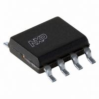
PCF85102C-2T/03,11 NXP Semiconductors, PCF85102C-2T/03,11 Datasheet - Page 6

PCF85102C-2T/03,11
Manufacturer Part Number
PCF85102C-2T/03,11
Description
IC EEPROM 2KBIT 100KHZ 8SOIC
Manufacturer
NXP Semiconductors
Datasheet
1.PCF85102C-2T0311.pdf
(20 pages)
Specifications of PCF85102C-2T/03,11
Memory Size
2K (256 x 8)
Package / Case
8-SOIC (3.9mm Width)
Format - Memory
EEPROMs - Serial
Memory Type
EEPROM
Speed
100kHz
Interface
I²C, 2-Wire Serial
Voltage - Supply
2.5 V ~ 6.0 V
Operating Temperature
-40°C ~ 85°C
Organization
256 K x 8
Interface Type
I2C
Maximum Clock Frequency
0.1 MHz
Supply Voltage (max)
6 V
Supply Voltage (min)
2.5 V
Maximum Operating Current
2 mA
Maximum Operating Temperature
+ 85 C
Mounting Style
SMD/SMT
Minimum Operating Temperature
- 40 C
Operating Supply Voltage
3.3 V, 5 V
Lead Free Status / RoHS Status
Lead free / RoHS Compliant
Lead Free Status / RoHS Status
Lead free / RoHS Compliant, Lead free / RoHS Compliant
Other names
935262037118
PCF85102C2D-T
PCF85102C2D-T
PCF85102C2D-T
PCF85102C2D-T
Philips Semiconductors
8. Functional description
9397 750 14216
Product data
8.1.1 Bus conditions
8.1.2 Data transfer
8.1 I
The I
serial bus consists of two bidirectional lines; one for data signals (SDA), and one for
clock signals (SCL).
Both the SDA and SCL lines must be connected to a positive supply voltage via a
pull-up resistor.
The following protocol has been defined:
The following bus conditions have been defined:
Bus not busy — Both data and clock lines remain HIGH.
Start data transfer — A change in the state of the data line, from HIGH-to-LOW,
while the clock is HIGH, defines the START condition.
Stop data transfer — A change in the state of the data line, from LOW-to-HIGH,
while the clock is HIGH, defines the STOP condition.
Data valid — The state of the data line represents valid data when, after a START
condition, the data line is stable for the duration of the HIGH period of the clock
signal. There is one clock pulse per bit of data.
Each data transfer is initiated with a START condition and terminated with a STOP
condition. The number of the data bytes, transferred between the START and STOP
conditions is limited to 7 bytes in the E/W mode and 8 bytes in the Page E/W mode.
Data transfer is unlimited in the read mode. The information is transmitted in bytes
and each receiver acknowledges with a ninth bit.
Within the I
fast-speed mode (400 kHz clock rate) are defined. The PCF85102C-2 operates in
only the standard-speed mode.
By definition, a device that sends a signal is called a ‘transmitter’, and the device
which receives the signal is called a ‘receiver’. The device which controls the signal is
called the ‘master’. The devices that are controlled by the master are called ‘slaves’.
Each byte is followed by one acknowledge bit. This acknowledge bit is a HIGH level,
put on the bus by the transmitter. The master generates an extra acknowledge related
clock pulse. The slave receiver which is addressed is obliged to generate an
acknowledge after the reception of each byte.
2
•
•
C-bus protocol
Data transfer may be initiated only when the bus is not busy.
During data transfer, the data line must remain stable whenever the clock line is
HIGH. Changes in the data line while the clock line is HIGH will be interpreted as
control signals.
2
C-bus is for 2-way, 2-line communication between different ICs or modules. The
2
C-bus specifications, a standard-speed mode (100 kHz clock rate) and a
Rev. 04 — 22 October 2004
256
8-bit CMOS EEPROM with I
© Koninklijke Philips Electronics N.V. 2004. All rights reserved.
PCF85102C-2
2
C-bus interface
6 of 20


