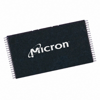
MT28F004B5VG-8 TET TR Micron Technology Inc, MT28F004B5VG-8 TET TR Datasheet - Page 8

MT28F004B5VG-8 TET TR
Manufacturer Part Number
MT28F004B5VG-8 TET TR
Description
IC FLASH 4MBIT 80NS 40TSOP
Manufacturer
Micron Technology Inc
Datasheet
1.MT28F004B5VG-8_B.pdf
(32 pages)
Specifications of MT28F004B5VG-8 TET TR
Format - Memory
FLASH
Memory Type
FLASH - Nor
Memory Size
4M (512K x 8)
Speed
80ns
Interface
Parallel
Voltage - Supply
4.5 V ~ 5.5 V
Operating Temperature
-40°C ~ 85°C
Package / Case
40-TSOP
Lead Free Status / RoHS Status
Contains lead / RoHS non-compliant
tional error information is set in three other bits: V
status, write status, and erase status.
Command Execution Logic (CEL)
device. These commands control the operation of the
ISM and the read path (i.e., memory array, ID register
or status register). Commands may be issued to the
CEL while the ISM is active. However, there are restric-
tions on what commands are allowed in this condition.
See the Command Execution section for more detail.
Deep Power-down Mode
MT28F004B5 and MT28F400B5 feature a very low cur-
rent, deep power-down mode. To enter this mode, the
RP# pin is taken to V
draw is a maximum of 20µA at 5V V
power-down also clears the status register and sets the
ISM to the read array mode.
MEMORY ARCHITECTURE
architecture is designed to allow sections to be erased
without disturbing the rest of the array. The array is
divided into seven addressable blocks that vary in size
and are independently erasable. When blocks rather
than the entire array are erased, total device endur-
ance is enhanced, as is system flexibility. Only the
ERASE function is block-oriented. All READ and
WRITE operations are done on a random-access basis.
ERASE or WRITE operations with a hardware protec-
tion circuit that requires a super-voltage be applied to
RP# or that the WP# pin be driven HIGH before erasure
is commenced. The boot block is intended for the core
firmware required for basic system functionality. The
09005aef8075d1f1
MT28F004B5.fm - Rev. 4, Pub. 2/2004
The CEL receives and interprets commands to the
To allow for maximum power conservation, the
The MT28F004B5 and MT28F400B5 memory array
The boot block is protected from unintentional
SS
±0.2V. In this mode, the current
CC
. Entering deep
SMART 5 BOOT BLOCK FLASH MEMORY
PP
8
remaining six blocks do not require that either of these
two conditions be met before WRITE or ERASE opera-
tions.
Boot Block
security for the most sensitive portions of the firm-
ware. This 16KB block may only be erased or written
when the RP# pin is at the specified boot block unlock
voltage (V
WRITE or ERASE of the boot block, the RP# pin must
be held at V
ERASE or WRITE is completed. The V
V
two configurations and top or bottom boot block. The
top boot block version supports processors of the x86
variety. The bottom boot block version is intended for
680X0 and RISC applications. Figure 1 illustrates the
memory address maps associated with these two ver-
sions.
Parameter Blocks
and more frequently changing system parameters and
also may store configuration or diagnostic coding.
These blocks are enabled for erasure when the V
is at V
required.
Main Memory Blocks
memory blocks and do not require a super-voltage on
RP# or WP# control to be erased or written. These
blocks are intended for code storage, ROM-resident
applications or operating systems that require in-sys-
tem update capability.
PPH
The hardware-protected boot block provides extra
The MT28F004B5 and MT28F400B5 are available in
The two 8KB parameter blocks store less sensitive
The four remaining blocks are general-purpose
(5V) when the boot block is written to or erased.
Micron Technology, Inc., reserves the right to change products or specifications without notice.
PPH
. No super-voltage unlock or WP# control is
HH
HH
) or when the WP# pin is V
or the WP# pin held HIGH until the
PP
©2002 Micron Technology, Inc.
pin must be at
IH
. During a
4Mb
PP
pin


