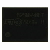
M29W640FT70ZA6E NUMONYX, M29W640FT70ZA6E Datasheet - Page 19

M29W640FT70ZA6E
Manufacturer Part Number
M29W640FT70ZA6E
Description
IC FLASH 64MBIT 70NS 48TFBGA
Manufacturer
NUMONYX
Series
Axcell™r
Datasheet
1.M29W640FB70ZA6E.pdf
(71 pages)
Specifications of M29W640FT70ZA6E
Format - Memory
FLASH
Memory Type
FLASH - Nor
Memory Size
64M (8Mx8, 4Mx16)
Speed
70ns
Interface
Parallel
Voltage - Supply
2.7 V ~ 3.6 V
Operating Temperature
-40°C ~ 85°C
Package / Case
48-TFBGA
Package
48TFBGA
Cell Type
NOR
Density
64 Mb
Architecture
Sectored
Block Organization
Asymmetrical
Location Of Boot Block
Top
Typical Operating Supply Voltage
3|3.3 V
Sector Size
8KByte x 8|64KByte x 127
Timing Type
Asynchronous
Interface Type
Parallel
Lead Free Status / RoHS Status
Lead free / RoHS Compliant
Other names
497-5034
497-5034
497-5034
Available stocks
Company
Part Number
Manufacturer
Quantity
Price
Company:
Part Number:
M29W640FT70ZA6E
Manufacturer:
Micron Technology Inc
Quantity:
10 000
4.1.3
4.1.4
Read CFI Query command
The Read CFI Query Command is used to read data from the Common Flash Interface
(CFI) Memory Area. This command is valid when the device is in the Read Array mode, or
when the device is in Autoselected mode.
One Bus Write cycle is required to issue the Read CFI Query Command. Once the
command is issued subsequent Bus Read operations read from the Common Flash
Interface Memory Area.
The Read/Reset command must be issued to return the device to the previous mode (the
Read Array mode or Autoselected mode). A second Read/Reset command would be
needed if the device is to be put in the Read Array mode from Autoselected mode.
See
on the information contained in the Common Flash Interface (CFI) memory area.
Chip Erase command
The Chip Erase command can be used to erase the entire chip. Six Bus Write operations
are required to issue the Chip Erase Command and start the Program/Erase Controller.
If any blocks are protected then these are ignored and all the other blocks are erased. If all
of the blocks are protected the Chip Erase operation appears to start but will terminate
within about 100μs, leaving the data unchanged. No error condition is given when protected
blocks are ignored.
During the erase operation the memory will ignore all commands, including the Erase
Suspend command. It is not possible to issue any command to abort the operation. Typical
chip erase times are given in
Endurance
Status Register on the Data Inputs/Outputs. See the section on the Status Register for more
details.
After the Chip Erase operation has completed the memory will return to the Read Mode,
unless an error has occurred. When an error occurs the memory will continue to output the
Status Register. A Read/Reset command must be issued to reset the error condition and
return to Read Mode.
The Chip Erase Command sets all of the bits in unprotected blocks of the memory to ’1’. All
previous data is lost.
Appendix B: Common Flash Interface
cycles. All Bus Read operations during the Chip Erase operation will output the
Table 8: Program, Erase times and Program, Erase
(CFI), Tables 23, 24, 25, 26,
27
and
28
for details
19/71


