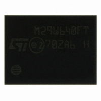
M29W640FT70ZA6E NUMONYX, M29W640FT70ZA6E Datasheet - Page 24

M29W640FT70ZA6E
Manufacturer Part Number
M29W640FT70ZA6E
Description
IC FLASH 64MBIT 70NS 48TFBGA
Manufacturer
NUMONYX
Series
Axcell™r
Datasheet
1.M29W640FB70ZA6E.pdf
(71 pages)
Specifications of M29W640FT70ZA6E
Format - Memory
FLASH
Memory Type
FLASH - Nor
Memory Size
64M (8Mx8, 4Mx16)
Speed
70ns
Interface
Parallel
Voltage - Supply
2.7 V ~ 3.6 V
Operating Temperature
-40°C ~ 85°C
Package / Case
48-TFBGA
Package
48TFBGA
Cell Type
NOR
Density
64 Mb
Architecture
Sectored
Block Organization
Asymmetrical
Location Of Boot Block
Top
Typical Operating Supply Voltage
3|3.3 V
Sector Size
8KByte x 8|64KByte x 127
Timing Type
Asynchronous
Interface Type
Parallel
Lead Free Status / RoHS Status
Lead free / RoHS Compliant
Other names
497-5034
497-5034
497-5034
Available stocks
Company
Part Number
Manufacturer
Quantity
Price
Company:
Part Number:
M29W640FT70ZA6E
Manufacturer:
Micron Technology Inc
Quantity:
10 000
4.2.3
4.2.4
2. For devices with process technology code “H” in the marking, the Double Word Program command can be performed
24/71
without applying V
Octuple Byte Program command
This is used to write eight adjacent Bytes, in x8 mode, simultaneously. The addresses of the
eight Bytes must differ only in A1, A0 and DQ15A-1.
Nine bus write cycles are necessary to issue the command:
1.
2.
3.
4.
5.
6.
7.
8.
9.
To perform the Quadruple Byte Program command, it is necessary to apply V
V
Double Word Program command
The Double Word Program command is used to write a page of two adjacent Words in
parallel. The two Words must differ only for the address A0.
Three bus write cycles are necessary to issue the Double Word Program command.
After the program operation has completed the memory will return to the Read mode, unless
an error has occurred. When an error occurs Bus Read operations will continue to output
the Status Register. A Read/Reset command must be issued to reset the error condition and
return to Read mode.
Note that the Fast Program commands cannot change a bit set at ’0’ back to ’1’. One of the
Erase Commands must be used to set all the bits in a block or in the whole memory from ’0’
to ’1’.
Typical Program times are given in
Endurance
PP
/WP pin.
The first bus cycle sets up the command.
The second bus cycle latches the Address and the Data of the first Byte to be written.
The third bus cycle latches the Address and the Data of the second Byte to be written.
The fourth bus cycle latches the Address and the Data of the third Byte to be written.
The fifth bus cycle latches the Address and the Data of the fourth Byte to be written.
The sixth bus cycle latches the Address and the Data of the fifth Byte to be written.
The seventh bus cycle latches the Address and the Data of the sixth Byte to be written.
The eighth bus cycle latches the Address and the Data of the seventh Byte to be
written.
The ninth bus cycle latches the Address and the Data of the eighth Byte to be written
and starts the Program/Erase Controller.
The first bus cycle sets up the Quadruple Word Program Command.
The second bus cycle latches the Address and the Data of the first Word to be written.
The third bus cycle latches the Address and the Data of the second Word to be written
and starts the Program/Erase Controller.
PPH
on the V
cycles.
PP
/WP pin. For other devices, applying V
Table 8: Program, Erase times and Program, Erase
(2)
PPH
on the V
PP
/WP pin is mandatory.
PPH
to the


