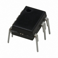
FSD210 Fairchild Semiconductor, FSD210 Datasheet - Page 9

FSD210
Manufacturer Part Number
FSD210
Description
IC SWIT PWM GREEN UVLO HV 7DIP
Manufacturer
Fairchild Semiconductor
Datasheet
1.FSD210.pdf
(18 pages)
Specifications of FSD210
Output Isolation
Isolated
Frequency Range
126 ~ 142kHz
Voltage - Input
6.7 ~ 20 V
Voltage - Output
700V
Power (watts)
7W
Operating Temperature
25°C ~ 100°C
Package / Case
8-DIP (0.300", 7.62mm), 7 Leads
Lead Free Status / RoHS Status
Lead free / RoHS Compliant
Other names
FSD210_NL
FSD210_NL
FSD210_NL
Available stocks
Company
Part Number
Manufacturer
Quantity
Price
Company:
Part Number:
FSD210
Manufacturer:
FAIRCHILD
Quantity:
10 000
Company:
Part Number:
FSD210
Manufacturer:
Fairchi/ON
Quantity:
23 000
Part Number:
FSD210
Manufacturer:
FAIRCHILD/仙童
Quantity:
20 000
Company:
Part Number:
FSD210B
Manufacturer:
FSC
Quantity:
5 600
Part Number:
FSD210B
Manufacturer:
ON/安森美
Quantity:
20 000
Company:
Part Number:
FSD210BH
Manufacturer:
TI
Quantity:
1 001
Part Number:
FSD210BM
Manufacturer:
FAIRCHILD/仙童
Quantity:
20 000
Company:
Part Number:
FSD210H
Manufacturer:
Fairchild
Quantity:
16 686
Part Number:
FSD210H
Manufacturer:
FAIRCHILD/仙童
Quantity:
20 000
Functional Description
1. Startup : At startup, the internal high voltage current
source supplies the internal bias and charges the external
Vcc capacitor as shown in figure 7. In the case of the
FSD210, when Vcc reaches 8.7V the device starts switching
and the internal high voltage current source is disabled (see
figure 1). The device continues to switch provided that Vcc
does not drop below 6.7V. For FSD210, after startup, the
bias is supplied from the auxiliary transformer winding. In
the case of FSD200, Vcc is continuously supplied from the
external high voltage source and Vcc is regulated to 7V by
an internal high voltage regulator (HVReg), thus eliminating
the need for an auxiliary winding (see figure 2).
Calculating the Vcc capacitor is an important step to design-
ing in the FSD200/210. At initial start-up in both the
FSD200/210, the stand-by maximum current is 100uA, sup-
plying current to UVLO and Vref Block. The charging cur-
rent (i) of the Vcc capacitor is equal to Istr - 100uA. After
Vcc reaches the UVLO start voltage only the bias winding
supplies Vcc current to device. When the bias winding volt-
age is not sufficient, the Vcc level decreases to the UVLO
stop voltage. At this time Vcc oscillates. In order to prevent
this ripple it is recommended that the Vcc capacitor be sized
between 10uF and 47uF.
2. Feedback Control : The FSD200/210 are both voltage
mode devices as shown in Figure 8. Usually, a H11A817
optocoupler and KA431 voltage reference (or a FOD2741
integrated optocoupler and voltage reference) are used to
implement the isolated secondary feedback network. The
feedback voltage is compared with an internally generated
sawtooth waveform, directly controlling the duty cycle.
When the KA431 reference pin voltage exceeds the internal
reference voltage of 2.5V, the optocoupler LED current
increases pulling down the feedback voltage and reducing
the duty cycle. This event will occur when either the input
voltage increases or the output load decreases.
Vin,dc
Vcc
Figure 6. Internal startup circuit
8.7V/
6.7V
L
FSD210
H
Istr
Vstr
Vin,dc
Vcc
7V
Istr
Reg.
HV
FSD200
Vstr
3. Leading edge blanking (LEB) : At the instant the inter-
nal Sense FET is turned on, there usually exists a high cur-
rent spike through the Sense FET, caused by the primary side
capacitance and secondary side rectifier diode reverse recov-
ery. Exceeding the pulse-by-pulse current limit could cause
premature termination of the switching pulse (see Protection
Section). To counter this effect, the FPS employs a leading
edge blanking (LEB) circuit. This circuit inhibits the over
current comparator for a short time (TLEB) after the Sense
FET is turned on.
4. Protection Circuit : The FSD200/210 has 2 self protec-
tion functions: over load protection (OLP) and thermal shut-
down (TSD). Because these protection circuits are fully
integrated into the IC with no external components, system
Vo
Figure 7. Charging the Vcc capacitor through Vstr
UVLO
UVLO
Vcc
start
stop
KA431
Figure 8. PWM and feedback circuit
i = I s t r - m a x 1 0 0 u A
i = I s t r - m a x 1 0 0 u A
i = I s t r - m a x 1 0 0 u A
i = I s t r - m a x 1 0 0 u A
i = I s t r - m a x
i = I s t r - m a x
i = I s t r - m a x
i = I s t r - m a x
Vfb
Vin,dc
Vin,dc
Vin,dc
Vin,dc
1 0 0 u A
1 0 0 u A
1 0 0 u A
1 0 0 u A
Cfb
FB
4
Vcc
Vcc
Vcc
Vcc
5uA
V
Vcc
SD
Vref
100uA
100uA
100uA
100uA
0.25mA
max
max
max
max
Auxiliary winding
Vcc must not drop
R
to UVLO stop
UVLO
voltage
Vref
Istr
Istr
Istr
Istr
Vstr
Vstr
Vstr
Vstr
OSC
J-FET
J-FET
J-FET
J-FET
OLP
FSD2xx
FSD2xx
FSD2xx
FSD2xx
FSD210, FSD200
driver
Gate
t
9


