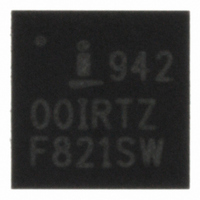
ISL94200IRZ Intersil, ISL94200IRZ Datasheet - Page 21

ISL94200IRZ
Manufacturer Part Number
ISL94200IRZ
Description
IC MULTI LI-ION OC PROT 24-QFN
Manufacturer
Intersil
Datasheet
1.ISL94200IRZ.pdf
(28 pages)
Specifications of ISL94200IRZ
Function
Over/Under Voltage Protection
Battery Type
Lithium-Ion (Li-Ion)
Voltage - Supply
5 V ~ 10 V
Operating Temperature
-40°C ~ 85°C
Mounting Type
Surface Mount
Package / Case
24-VFQFN Exposed Pad
Lead Free Status / RoHS Status
Lead free / RoHS Compliant
Available stocks
Company
Part Number
Manufacturer
Quantity
Price
Company:
Part Number:
ISL94200IRZ
Manufacturer:
Intersil
Quantity:
20
External VMON/CFET Protection Mechanisms
When there is a single charge/discharge path, a blocking
diode is recommended in the VMON to P- path in ISL94200
solution. See D
a negative voltage on the VMON pin that can occur when the
FETs are off and the charger connects to the pack. This
diode is not needed when there is a separate charge and
discharge path, because the voltages on P- (discharge) are
likely always positive. The diode also is not needed if the
differential between the minimum pack voltage and
maximum charger voltage does not exceed 22V.
When the pack is designed with a single set of
charge/discharge FETs, the ISL94200 CFET pin should be
protected in the event of an over-current or short circuit
shutdown. When this happens, the FET opens suddenly.
The flyback voltage from the motor windings could exceed
the maximum input voltage on the CFET pin. So, it is
recommended that an additional external series diode be
placed between the CFET pin of the ISL94200 and the gate
of the Charge FET. See Diode D
reduce the CFET gate voltage, but not significantly.
Finally, to protect the Charge FET itself in the event of a
large negative voltage on the Pack- pin, zener diode D
added. The large negative voltage can occur when the P- pin
goes significantly negative, while the CFET pin is being
internally clamped at VSS. The zener voltage of D4 should
be less than the V
User Flags
The ISL94200 contains four flags in the register area that the
microcontroller can use for general purpose indicators.
These bits are designated UFLG3, UFLG2, UFLG1, and
UFLG0. The microcontroller can set or reset these bits by
writing into the appropriate register.
The user flag bits are battery backed up, so the contents
remain even after exiting a sleep mode. However, if the
FIGURE 7. USE OF A DIODES FOR PROTECTING THE CFET
AND VMON PINS
1
ISL94200
in Figure 7. This diode is to protect against
VMON
GS
CFET
DFET
(max) specification of the FET.
21
D
3
3
D
10M
1
in Figure 7. This will
1M
D
4
PACK+
PACK-
4
is
ISL94200
microcontroller sets the POR bit to force a power on reset, all
of the user flags will also be reset. In addition, if the voltage
on cell-1 ever drops below the POR voltage, the contents of
the user flags (as well as all other register values) could be
lost.
Serial Interface
INTERFACE CONVENTIONS
The device supports a bidirectional bus oriented protocol.
The protocol defines any device that sends data onto the
bus as a transmitter, and the receiving device as the
receiver. The device controlling the transfer is called the
master and the device being controlled is called the slave.
The master always initiates data transfers, and provides the
clock for both transmit and receive operations. Therefore,
the ISL94200 devices operate as slaves in all applications.
When sending or receiving data, the convention is the most
significant bit (MSB) is sent first. So, the first address bit sent
is Bit 7.
CLOCK AND DATA
Data states on the SDA line can change only while SCL is
LOW. SDA state changes during SCL HIGH are reserved for
indicating start and stop conditions. See Figure 8.
START CONDITION
All commands are preceded by the start condition, which is a
HIGH to LOW transition of SDA when SCL is HIGH. The
device continuously monitors the SDA and SCL lines for the
start condition and will not respond to any command until
this condition has been met. See Figure 9.
STOP CONDITION
All communications must be terminated by a stop condition,
which is a LOW to HIGH transition of SDA when SCL is
HIGH. The stop condition is also used to place the device
into the Standby power mode after a read sequence. A stop
condition is only issued after the transmitting device has
released the bus. See Figure 9.
ACKNOWLEDGE
Acknowledge is a software convention used to indicate
successful data transfer. The transmitting device, either
master or slave, releases the bus after transmitting eight
bits. During the ninth clock cycle, the receiver pulls the SDA
line LOW to acknowledge that it received the eight bits of
data. See Figure 10.
The device responds with an acknowledge after recognition
of a start condition and the correct slave byte. If a write
operation is selected, the device responds with an
acknowledge after the receipt of each subsequent eight bits.
The device acknowledges all incoming data and address
bytes, except for the slave byte when the contents do not
match the device’s internal slave address.
July 3, 2008
FN6718.0


