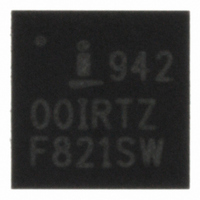
ISL94200IRZ Intersil, ISL94200IRZ Datasheet - Page 7

ISL94200IRZ
Manufacturer Part Number
ISL94200IRZ
Description
IC MULTI LI-ION OC PROT 24-QFN
Manufacturer
Intersil
Datasheet
1.ISL94200IRZ.pdf
(28 pages)
Specifications of ISL94200IRZ
Function
Over/Under Voltage Protection
Battery Type
Lithium-Ion (Li-Ion)
Voltage - Supply
5 V ~ 10 V
Operating Temperature
-40°C ~ 85°C
Mounting Type
Surface Mount
Package / Case
24-VFQFN Exposed Pad
Lead Free Status / RoHS Status
Lead free / RoHS Compliant
Available stocks
Company
Part Number
Manufacturer
Quantity
Price
Company:
Part Number:
ISL94200IRZ
Manufacturer:
Intersil
Quantity:
20
Operating Specifications
Internal Temperature Monitor Output
AO Output Stabilization Time
WAKE UP/SLEEP SPECIFICATIONS
Device WKUP Pin Voltage Threshold
(WKUP Pin Active High - Rising Edge)
Device Wkup Pin Hysteresis
(WKUP Pin Active High)
Input Resistance On WKUP
Device WKUP Pin Active Voltage
Threshold (WKUP Pin Active Low -
Falling Edge)
Device Wkup Pin Hysteresis
(WKUP Pin Active Low)
Device Wake-up Delay
FET CONTROL SPECIFICATIONS (FOR VCELL1, VCELL2, VCELL3 VOLTAGES FROM 2.8V TO 4.3V)
Control Outputs Response Time
(CFET, DFET)
CFET Gate Voltage
DFETGate Voltage
FET Turn On Current (DFET)
FET Turn On Current (CFET)
FET Turn Off Current (DFET)
DFET Resistance to VSS
SERIAL INTERFACE CHARACTERISTICS
SCL Clock Frequency
Pulse Width Suppression Time at
SDA and SCL Inputs
SCL Falling Edge to SDA Output Data
Valid
Time the Bus Must Be Free Before
Start of New Transmission
Clock Low Time
Clock High Time
PARAMETER
7
Over the recommended operating conditions unless otherwise specified. Parameters with MIN and/or MAX
limits are 100% tested at +25°C, unless otherwise specified. Temperature limits established by characterization
and are not production tested. (Continued)
V
V
R
SYMBOL
V
V
I
R
I
VCFET
VDFET
DF(OFF)
WKUP1H
WKUP2H
T
t
I
CF(ON)
DF(OFF)
WKUP1
WKUP2
t
WKUP
DFON
t
t
t
WKUP
f
HIGH
INT25
t
LOW
VSC
t
BUF
SCL
t
CO
AA
IN
Output at +25°C
From SCL falling edge at data bit 0 of
command to AO output stable within 0.5%
of final value. AO voltage steps from 0V to
2V. (C
WKUP pin rising edge (WKPOL = 1)
Device wakes up and sets WKUP flag
HIGH.
WKUP pin falling edge hysteresis
(WKPOL = 1) sets WKUP flag LOW (does
not automatically enter sleep mode)
Resistance from WKUP pin to VSS
(WKPOL = 1)
WKUP pin falling edge (WKPOL = 0)
Device wakes up and sets WKUP flag
HIGH.
WKUP pin rising edge hysteresis
(WKPOL = 0) sets WKUP flag LOW (does
not automatically enter sleep mode)
Delay after voltage on WKUP pin crosses
the threshold (rising or falling) before
activating the WKUP bit.
Bit 0 to start of control signal (DFET) Bit 1
to start of control signal (CFET)
No load on CFET
No load on DFET
DFET voltage = 0 to VCELL3 -1.5V
CFET voltage = 0 to VCELL3 - 1.5V
DFET voltage = VDFET to 1V
VDFET <1V (When turning off the FET)
Any pulse narrower than the max spec is
suppressed.
From SCL falling crossing V
SDA exits the V
window.
SDA crossing V
condition to SDA crossing V
the following START condition.
Measured at the V
Measured at the V
AO
= 10pF) (Note 7)
TEST CONDITION
ISL94200
IL
IH
(max) to V
(min) during a STOP
IL
IH
(max) crossing.
(min) crossing.
IH
IH
IH
(min) during
(min)
(min), until
V
V
V
CELL1
CELL3
CELL3
MIN
130
100
3.5
4.7
4.7
4.0
20
80
80
- 2.6 V
- 0.5
- 0.5
CELL1
TYP
1.31
100
230
200
130
200
180
5.0
1.0
40
- 2.0 V
V
V
CELL3
CELL3
CELL1
MAX
330
400
400
100
0.1
6.5
3.5
60
11
50
+ 0.1
+ 0.1
- 1.2
July 3, 2008
FN6718.0
UNIT
kHz
mV
mV
mA
ms
ms
kΩ
µA
µA
µs
ns
µs
µs
µs
µs
Ω
V
V
V
V
V


