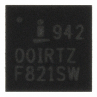
ISL94200IRZ Intersil, ISL94200IRZ Datasheet - Page 8

ISL94200IRZ
Manufacturer Part Number
ISL94200IRZ
Description
IC MULTI LI-ION OC PROT 24-QFN
Manufacturer
Intersil
Datasheet
1.ISL94200IRZ.pdf
(28 pages)
Specifications of ISL94200IRZ
Function
Over/Under Voltage Protection
Battery Type
Lithium-Ion (Li-Ion)
Voltage - Supply
5 V ~ 10 V
Operating Temperature
-40°C ~ 85°C
Mounting Type
Surface Mount
Package / Case
24-VFQFN Exposed Pad
Lead Free Status / RoHS Status
Lead free / RoHS Compliant
Available stocks
Company
Part Number
Manufacturer
Quantity
Price
Company:
Part Number:
ISL94200IRZ
Manufacturer:
Intersil
Quantity:
20
Operating Specifications
NOTES:
Start Condition Setup Time
Start Condition Hold Time
Input Data Setup Time
Input Data Hold Time
Stop Condition Setup Time
Stop Condition Hold Time
Data Output Hold Time
SDA and SCL Rise Time
SDA and SCL Fall Time
Capacitive Loading Of SDA Or SCL
(Note 5)
SDA and SCL Bus Pull-up Resistor-
Off-Chip (Note 5)
Input Leakage Current (SCL, SDA)
Input Buffer Low Voltage (SCL, SDA)
Input Buffer High Voltage (SCL, SDA)
Output Buffer Low Voltage (SDA)
SDA and SCL Input Buffer Hysteresis
(Note 5)
3. Power-up of the device requires all V
4. The device provides an internal hold time of at least 300ns for the SDA signal to bridge the unidentified region of the falling edge of SCL.
5. Limits should be considered typical and are not production tested.
6. Typical 5Ω ±2Ω, based on characterization data.
7. Maximum output capacitance = 15pF.
PARAMETER
8
Over the recommended operating conditions unless otherwise specified. Parameters with MIN and/or MAX
limits are 100% tested at +25°C, unless otherwise specified. Temperature limits established by characterization
and are not production tested. (Continued)
SYMBOL
I
t
t
2
t
t
t
t
HD:DAT
SU:STO
HD:STO
SU:STA
HD:STA
SU:DAT
CELL1
R
CHYST Sleep bit = 0
V
t
V
V
Cb
OUT
I
DH
t
t
LI
OL
R
F
IH
IL
, V
CELL2
SCL rising edge to SDA falling edge. Both
crossing the V
From SDA falling edge crossing V
to SCL falling edge crossing V
From SDA exiting the V
window to SCL rising edge crossing
V
From SCL falling edge crossing V
to SDA entering the V
window.
From SCL rising edge crossing V
SDA rising edge crossing V
From SDA rising edge to SCL falling edge.
Both crossing V
From SCL falling edge crossing V
until SDA enters the V
window. (Note 4)
From V
From V
Total on-chip and off-chip
Maximum is determined by t
For C
For C
Voltage relative to V
Voltage relative to V
I
OL
IL
(min).
= 1mA
B
B
, V
IL
IH
= 400pF, max is about 2kΩ ~ 2.5kΩ
= 40pF, max is about 15kΩ to 20kΩ
CELL3
(max) to V
(min) to V
TEST CONDITION
IH
, and VCC to be above the limits specified.
ISL94200
IH
(min) level.
(min).
IL
IH
SS
SS
(max).
(min).
IL
IL
IL
of the device.
of the device.
(max) to V
(max) to V
(max) to V
IL
R
(max).
IH
and t
(min).
IH
IH
IL
IL
IH
(min) to
IH
IH
(max)
F
(max)
(min)
(min)
.
(min)
(min)
0.05 * V
V
RGO
MIN
250
300
-0.3
-10
4.7
4.0
4.0
4.0
0
1
x 0.7
RGO
TYP
V
V
RGO
RGO
MAX
1000
300
400
0.4
10
+ 0.1
x 0.3
July 3, 2008
FN6718.0
UNIT
pF
kΩ
µA
µs
µs
ns
µs
µs
µs
ns
ns
ns
V
V
V
V


