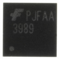
FAN3989MLP8X Fairchild Semiconductor, FAN3989MLP8X Datasheet

FAN3989MLP8X
Specifications of FAN3989MLP8X
Available stocks
Related parts for FAN3989MLP8X
FAN3989MLP8X Summary of contents
Page 1
... Handheld Devices Related Resources AN-5067 — PCB Land Pattern Design and Surface Mount Guidelines for MLP Packages Ordering Information Operating Part Number Temperature Range FAN3989MLP8X -40°C to +85°C V BUS D- D+ GND © 2007 Fairchild Semiconductor Corporation FAN3989 Rev. 1.0.8 ...
Page 2
... GT 6V BUS V LT 3.3V LT 3.3V BUS PC Charger 5V © 2007 Fairchild Semiconductor Corporation FAN3989 • Rev. 1.0.8 Figure 3. Description USB Data Input Device Ground Over-/Under-Voltage Flag Output PMOS Switch Control – Pull-Up Connection to V Voltage Out – Connection also on Package DAP (see PCB Layout Guideline ...
Page 3
... Fairchild does not recommend exceeding them or designing to Absolute Maximum Ratings. Symbol T Operating Temperature Range A V Supply Voltage Range CC © 2007 Fairchild Semiconductor Corporation FAN3989 • Rev. 1.0.8 Parameter Parameter Min. Parameter Parameter Min. 3 Min ...
Page 4
... Drain Source Breakdown VB DSS Voltage Static Drain-Source On R DSON Resistance C Input Capacitance iss C Output Capacitance oss t PMOS Turn-On Delay Time d(on) t PMOS Turn-Off Delay Time d(off) © 2007 Fairchild Semiconductor Corporation FAN3989 • Rev. 1.0.8 Conditions V Range +5.0V Shorted +5.0V Shorted BUS ...
Page 5
... Typical Performance Characteristics V = 2.7V-7.0V CC 1.00 0.90 0.80 0.70 0.60 0.50 0. Figure 4. I vs. V (2.7V-7.0V) No Load CC CC © 2007 Fairchild Semiconductor Corporation FAN3989 • Rev. 1.0.8 1.8 1.6 1.4 1.2 Icc 1 0.8 0.6 0.4 Figure 192.0 190.0 188.0 186.0 184.0 182.0 180.0 ...
Page 6
... Typical Performance Characteristics © 2007 Fairchild Semiconductor Corporation FAN3989 • Rev. 1.0.8 (Continued) Figure 8. Turn-Off Time Figure 9. No Fault on Flag 1, Skew=65ns 6 www.fairchildsemi.com ...
Page 7
... Typical Performance Characteristics Figure 10. © 2007 Fairchild Semiconductor Corporation FAN3989 • Rev. 1.0.8 (Continued) PC Data Running D+/D- (Flag 1 and Flag 2 at Correct Levels) Figure 11. Standard USB Charger Plug-In 7 www.fairchildsemi.com ...
Page 8
... PMOS switch standard USB configuration, there is a switch in the USB transceiver that is always on in full-speed mode during the transition from full-speed to high-speed mode and turned off after enumeration is © 2007 Fairchild Semiconductor Corporation FAN3989 • Rev. 1.0 1.5K ...
Page 9
... D+ and D- inputs. A 5MΩ pull- down on the D- line and a 1MΩ pull- line are recommended charger is plugged into © 2007 Fairchild Semiconductor Corporation FAN3989 • Rev. 1.0.8 (Continued) LSctrl Comparato r ...
Page 10
... PCB Layout Guidelines Please also see Fairchild Semiconductor applications note AN-5067 — PCB Land Pattern Design and Surface Mount Guidelines for MLP Packages Pad1 This exposed DAP is connected to the internal FET drain and labeled V on the device. The pad should OUT be connected to V pin of the device or left floating ...
Page 11
... Package drawings are provided as a service to customers considering Fairchild components. Drawings may change in any manner without notice. Please note the revision and/or date on the drawing and contact a Fairchild Semiconductor representative to verify or obtain the most recent revision. Package specifications do not expand the terms of Fairchild’s worldwide terms and conditions, specifically the warranty therein, which covers Fairchild products. Always visit Fairchild Semiconductor’ ...
Page 12
... Fairchild Semiconductor Corporation FAN3989 • Rev. 1.0.8 12 www.fairchildsemi.com ...


