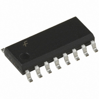
ML4824CS1 Fairchild Semiconductor, ML4824CS1 Datasheet - Page 9

ML4824CS1
Manufacturer Part Number
ML4824CS1
Description
IC PFC PWM CTRLR COMBO 16-SOIC
Manufacturer
Fairchild Semiconductor
Datasheet
1.ML4824IP1.pdf
(15 pages)
Specifications of ML4824CS1
Mode
Average Current
Frequency - Switching
76kHz
Current - Startup
700µA
Voltage - Supply
10.5 V ~ 13.2 V
Operating Temperature
0°C ~ 70°C
Mounting Type
Surface Mount
Package / Case
16-SOIC (0.300", 7.5mm Width)
Switching Frequency
81 KHz
Maximum Operating Temperature
+ 150 C
Mounting Style
SMD/SMT
Minimum Operating Temperature
- 65 C
Lead Free Status / RoHS Status
Lead free / RoHS Compliant
PRODUCT SPECIFICATION
ML4824’s voltage error amplifier has a specially shaped
nonlinearity such that under steady-state operating condi-
tions the transconductance of the error amplifier is at a local
minimum. Rapid perturbations in line or load conditions will
cause the input to the voltage error amplifier (V
ate from its 2.5V (nominal) value. If this happens, the
transconductance of the voltage error amplifier will increase
significantly, as shown in the Typical Performance Charac-
teristics. This raises the gain-bandwidth product of the volt-
age loop, resulting in a much more rapid voltage loop
response to such perturbations than would occur with a con-
ventional linear gain characteristic.
The current amplifier compensation is similar to that of the
voltage error amplifier with the exception of the choice of
crossover frequency. The crossover frequency of the current
amplifier should be at least 10 times that of the voltage
amplifier, to prevent interaction with the voltage loop. It
should also be limited to less than 1/6th that of the switching
frequency, e.g. 16.7kHz for a 100kHz switching frequency.
There is a modest degree of gain contouring applied to the
transfer characteristic of the current error amplifier, to
increase its speed of response to current-loop perturbations.
However, the boost inductor will usually be the dominant
factor in overall current loop response. Therefore, this con-
touring is significantly less marked than that of the voltage
error amplifier. This is illustrated in the Typical Performance
Characteristics.
For more information on compensating the current and
voltage control loops, see Application Notes 33 and 34.
Application Note 16 also contains valuable information for
the design of this class of PFC.
Oscillator (RAMP 1)
The oscillator frequency is determined by the values of R
and C
oscillator output clock:
The deadtime of the oscillator is derived from the following
equation:
at V
The deadtime of the oscillator may be determined using:
The deadtime is so small (t
operating frequency can typically be approximated by:
REV. 1.0.6 11/7/03
f
f
t
t
OSC
t
OSC
REF
RAMP
RAMP
DEADTIME
T
, which determine the ramp and off-time of the
= 7.5V:
=
=
=
=
--------------- -
t
-------------------------------------------------- -
t
RAMP
RAMP
C
C
1
T
T
=
----------------- -
5.1mA
R
+
R
2.5V
T
T
t
1
DEADTIME
In
0.51
V
------------------------------- -
V
RAMP
C
REF
REF
T
=
–
–
490 C
>> t
1.25
3.75
DEADTIME
T
FB
) that the
) to devi-
(3)
(4)
(5)
T
(2)
EXAMPLE:
For the application circuit shown in the data sheet, with the
oscillator running at:
Solving for R
components values, C
The deadtime of the oscillator adds to the Maximum PWM
Duty Cycle (it is an input to the Duty Cycle Limiter). With
zero oscillator deadtime, the Maximum PWM Duty Cycle is
typically 45%. In many applications, care should be taken
that C
Duty Cycle beyond 50%. This can be accomplished by using
a stable 470pF capacitor for C
PWM SECTION
Pulse Width Modulator
The PWM section of the ML4824 is straightforward, but
there are several points which should be noted. Foremost
among these is its inherent synchronization to the PFC
section of the device, from which it also derives its basic
timing (at the PFC frequency in the ML4824-1, and at twice
the PFC frequency in the ML4824-2). The PWM is capable
of current-mode or voltage mode operation. In current-mode
applications, the PWM ramp (RAMP 2) is usually derived
directly from a current sensing resistor or current trans-
former in the primary of the output stage, and is thereby
representative of the current flowing in the converter’s output
stage. DC I
limiting, is typically connected to RAMP 2 in such applica-
tions. For voltage-mode operation or certain specialized
applications, RAMP 2 can be connected to a separate RC
timing network to generate a voltage ramp against which
V
voltage feedforward from the PFC buss can assist in line
regulation accuracy and response. As in current mode
operation, the DC I
overcurrent protection.
No voltage error amplifier is included in the PWM stage of
the ML4824, as this function is generally performed on the
output side of the PWM’s isolation boundary. To facilitate
the design of optocoupler feedback circuitry, an offset has
been built into the PWM’s RAMP 2 input which allows V
to command a zero percent duty cycle for input voltages
below 1.25V.
PWM Current Limit
The DC I
current limiter for the PWM section. Should the input
voltage at this pin ever exceed 1V, the output of the PWM
will be disabled until the output flip-flop is reset by the clock
pulse at the start of the next PWM power cycle.
DC
f
t
RAMP
OSC
will be compared. Under these conditions, the use of
T
not be made so large as to extend the Maximum
LIMIT
=
=
LIMIT
100kHz
C
T
T
x C
pin is a direct input to the cycle-by-cycle
, which provides cycle-by-cycle current
R
T
LIMIT
T
yields 2 x 10
=
T
--------------- -
t
0.51
= 470pF, and R
RAMP
input is used for output stage
1
=
T
.
1 10
-4
. Selecting standard
–
5
T
= 41.2k .
ML4824
DC
9


