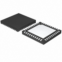
ISL97653AIRZ-TK Intersil, ISL97653AIRZ-TK Datasheet - Page 10

ISL97653AIRZ-TK
Manufacturer Part Number
ISL97653AIRZ-TK
Description
IC LCD SUPPLY 5CHN 40-QFN
Manufacturer
Intersil
Datasheet
1.ISL97653AIRZ.pdf
(18 pages)
Specifications of ISL97653AIRZ-TK
Applications
LCD TV/Monitor
Current - Supply
4mA
Voltage - Supply
4 V ~ 14 V
Operating Temperature
-40°C ~ 105°C
Mounting Type
Surface Mount
Package / Case
40-QFN
Lead Free Status / RoHS Status
Lead free / RoHS Compliant
Pin Descriptions
PIN NUMBER
32, 33
34, 35
25
26
27
28
29
30
31
36
37
38
39
40
PGND1, PGND2
PIN NAME
(Continued)
LDO-CTL
LX1, LX2
LDO-FB
COMP
AGND
PVIN1
CDEL
RSET
TEMP
PROT
HVS
FBB
EN
10
V
cap reaching µA levels.
Chip enable (active high). Can be driven to VIN levels.
High-voltage stress input select pin. High selects high voltage mode.
Voltage set pin for HVS test. RSET connects to ground in the high voltage mode - RSET high.
A
Boost compensation network pin. An RC network is recommended. Increase R for better transient
response at the expense of stability. R = 0Ω is recommended for 4.4A Boost requirements.
Temperature sensor output voltage. An analog voltage from 0V to 3V for temperatures of -40°C to
+150°C.
Boost ground pins.
Boost switch output. Drain of the internal power NMOS for the Boost.
Gate driver of the Input protection switch. Goes low when EN is high. Can be used to modulate the
passive input inrush current as shown by R
page 5.
Analog ground. Separate from PGND’s and star under the chip.
Logic buck supply voltage.This is also the analog supply from which the VL is generated. Needs at least
1µF bypassing.
LDO controller feedback. High impedance input to regulate at 1.215V.
LDO control pin. Gate drive for the external PNP BJT.
VDD
ON
slice control delay input. Minimum 47nF. Recommend 220nF but is only limited by leakage in the
boost feedback pin. High impedance input to regulate at 1.215V.
ISL97653A
DESCRIPTION
21
,R
22
, and C
30
in the “Typical Application Diagram” on
September 7, 2010
FN6367.3


