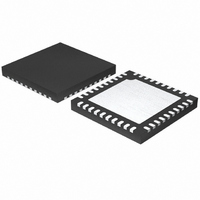
ISL97653AIRZ-TK Intersil, ISL97653AIRZ-TK Datasheet - Page 12

ISL97653AIRZ-TK
Manufacturer Part Number
ISL97653AIRZ-TK
Description
IC LCD SUPPLY 5CHN 40-QFN
Manufacturer
Intersil
Datasheet
1.ISL97653AIRZ.pdf
(18 pages)
Specifications of ISL97653AIRZ-TK
Applications
LCD TV/Monitor
Current - Supply
4mA
Voltage - Supply
4 V ~ 14 V
Operating Temperature
-40°C ~ 105°C
Mounting Type
Surface Mount
Package / Case
40-QFN
Lead Free Status / RoHS Status
Lead free / RoHS Compliant
Rectifier Diode (Boost Converter)
A high-speed diode is necessary due to the high switching
frequency. Schottky diodes are recommended because of
their fast recovery time and low forward voltage. The reverse
voltage rating of this diode should be higher than the
maximum output voltage. The rectifier diode must meet the
output current and peak inductor current requirements. The
following table lists two recommendations for boost
converter diode.
Output Capacitor
Integrating output capacitors supply the load directly and
reduce the ripple voltage at the output. Output ripple voltage
consists of two components: the voltage drop due to the
inductor ripple current flowing through the ESR of output
capacitor, and the charging and discharging of the output
capacitor.
For low ESR ceramic capacitors, the output ripple is
dominated by the charging and discharging of the output
capacitor. The voltage rating of the output capacitor should
be greater than the maximum output voltage.
Note: Capacitors have a voltage coefficient that makes their
effective capacitance drop as the voltage across them
increases. C
of the capacitor at a particular voltage and not the
manufacturer's stated value, measured at zero volts.
Table 5 shows some selections of output capacitors.
PI Loop Compensation (Boost Converter)
The boost converter of ISL97653A can be compensated by
a RC network connected from COMP pin to ground.
C
demo board. A higher capacitor value can be used to
increase system stability.
V
CAPACITOR
TABLE 5. BOOST OUTPUT CAPACITOR RECOMMENDATION
FYD0504SA
RIPPLE
2
30WQ04FN
10µF/25V
10µF/25V
TABLE 4. BOOST CONVERTER RECTIFIER DIODE
= 4.7nF and R
DIODE
=
I
LPK
RECOMMENDATION
OUT
SIZE
1210
1210
×
40V/3.5A
V
RATING
in Equation 7 assumes the effective value
2
50V/2A
ESR
R
= 0Ω to 10Ω. A RC network is used in the
/I
AVG
TDK
Murata
+
V
----------------------- -
O
VENDOR
V
–
O
12
V
PACKAGE
IN
DPAK
DPAK
×
--------------- -
C
OUT
I
O
GRM32DR61E106K
C3225X7R1E106M
×
Fairchild
Semiconductor
International
Rectifier
PART NUMBER
--- -
f
1
s
VENDOR
(EQ. 7)
ISL97653A
Stability can be examined by repeatedly changing the load
between 100mA and a max level that is likely to be used in
the system being used. The A
examined with an oscilloscope set to AC 100mV/DIV and the
amount of ringing observed when the load current changes.
Reduce excessive ringing by reducing the value of the
resistor in series with the CM1 pin capacitor.
Cascaded MOSFET Application
A 20V N-Channel MOSFET is integrated in the boost
regulator. For applications requiring output voltages greater
than 20V, an external cascaded MOSFET is needed as
shown in Figure 15. The voltage rating of the external
MOSFET should be greater than A
V
A series external P-FET can be used to prevent passive
power-up inrush current from the Boost output capacitors
charging to V
Schottky diode. This FET also adds protection in the event of
a short circuit on A
in the “Typical Application Diagram” on page 5) is controlled
by PROT. When EN is low, PROT is pulled internally to
PVIN1, thus M0 is switched off. When EN goes high, PROT
is pulled down slowly via a 50µA current source, switching
M0 on.
If the device is powered up with EN tied to high, M0 will
remain switched off until the voltage on VL exceeds the
VLOR threshold. Once the voltage on PROT falls below 0.6V
and the step-up regulator is within 90% of its target voltage,
PROT is pulled down to ground via a 1.3kΩ impedance. If
A
to a 50µA current source. If a timed fault is detected, M0 is
actively switched off.
Several additional external components can optionally be
used to fine-tune the function of pin PROT (shown in the
dashed box near M0 in the application diagram). PROT
ramp rate can be controlled by adding a capacitor C30
between gate and source of M0. M0 gate voltage can be
VDD
FIGURE 15. CASCADED MOSFET TOPOLOGY FOR HIGH
IN
V
IN
Protection
falls 10% below regulation, the drive to PROT reverts
IN
OUTPUT VOLTAGE APPLICATIONS
INTERSIL
ISL97653A
- V
VDD.
SCHOTTKY
The gate of the PFET (shown as M0
LX1, LX2
VDD
via the boost inductor and
FBB
voltage should be
VDD
.
September 7, 2010
FN6367.3
A
VDD


