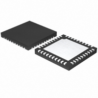
ISL97653AIRZ-TK Intersil, ISL97653AIRZ-TK Datasheet - Page 17

ISL97653AIRZ-TK
Manufacturer Part Number
ISL97653AIRZ-TK
Description
IC LCD SUPPLY 5CHN 40-QFN
Manufacturer
Intersil
Datasheet
1.ISL97653AIRZ.pdf
(18 pages)
Specifications of ISL97653AIRZ-TK
Applications
LCD TV/Monitor
Current - Supply
4mA
Voltage - Supply
4 V ~ 14 V
Operating Temperature
-40°C ~ 105°C
Mounting Type
Surface Mount
Package / Case
40-QFN
Lead Free Status / RoHS Status
Lead free / RoHS Compliant
When EN is taken high, voltage of pin PROT and V
ramping down. Once the PROT voltage falls below 0.9V,
A
V
connect to V
absolute value. The delay between V
controlled by C30 in the “Typical Application Diagram” on
page 5m and is given by Equation 23:
The successful completion of the A
triggers two simultaneous events. V
and the voltage on CDEL starts ramping up. When the
voltage reaches 1.215V, V
Temperature Sensor
The ISL97653A also includes a temperature output for use
in system thermal management control. The integrated
sensor measures the die temperature over the -40°C to
+150°C range. Output is in the form of an analog voltage on
the TEMP pin in the range of 0V to 3V, which is proportional
to the sensed die temperature. Temperature accuracy is
±8.5°C over the -40°C to +150°C temperature range.
The device should be disabled by the user when the TEMP
pin output reaches 3V ( = +150°C die junction). Operation of
the device between +125°C and +150°C can be tolerated for
short periods, however in order to maximize the life of the IC,
it is recommended that the effective continuous operating
junction temperature of the die should not exceed +125°C.
Intersil products are sold by description only. Intersil Corporation reserves the right to make changes in circuit design, software and/or specifications at any time without
notice. Accordingly, the reader is cautioned to verify that data sheets are current before placing orders. Information furnished by Intersil is believed to be accurate and
reliable. However, no responsibility is assumed by Intersil or its subsidiaries for its use; nor for any infringements of patents or other rights of third parties which may result
from its use. No license is granted by implication or otherwise under any patent or patent rights of Intersil or its subsidiaries.
t
DELAY
VDD
OFF
starts up with a 9ms fixed soft-start time. Please note if
is to start earlier than
=
(
V
V
ON
IN
IN
VREF
V
PROT
CDEL
Slice
A
LOGIC
V
V
, and V
All Intersil U.S. products are manufactured, assembled and tested utilizing ISO9000 quality systems.
–
EN
VDD
OFF
V
ON
IN
0.9V
* For demonstration only, not to scale
Intersil Corporation’s quality certifications can be viewed at www.intersil.com/design/quality
)
IN
×
For information regarding Intersil Corporation and its products, see www.intersil.com
C
voltage should be larger than V
FIGURE 18.
30
ON
⁄
A
(
17
VDD
50μA
slice starts.
0.9V
, then the SUPN needs to
)
VDD
ON
1.215V
OFF
begins to ramp up
soft-start cycle
2.8V
and
A
VDD
OFF
can be
(EQ. 23)
start
OFF
ISL97653A
Fault Sequencing
The ISL97653A has advanced overall fault detection
systems including Overcurrent Protection (OCP) for both
boost and buck converters, Undervoltage Lockout Protection
(UVLP) and Over-Temperature Protection.
Once the peak current flowing through the switching
MOSFET of the boost and buck converters triggers the
current limit threshold, the PWM comparator will disable the
output, cycle by cycle, until the current is back to normal.
Layout Recommendation
The device's performance including efficiency, output noise,
transient response and control loop stability is dramatically
affected by the PCB layout. PCB layout is critical, especially
at high switching frequency.
There are some general guidelines for layout:
A demo board is available to illustrate the proper layout
implementation.
1. Place the external power components (the input
2. Place V
3. Reduce the loop with large AC amplitudes and fast slew
4. The feedback network should sense the output voltage
5. The power ground (PGND) and signal ground (SGND)
6. The exposed die plate, on the underneath of the
7. To minimize the thermal resistance of the package when
8. Minimize feedback input track lengths to avoid switching
capacitors, output capacitors, boost inductor and output
diodes, etc.) in close proximity to the device. Traces to
these components should be kept as short and wide as
possible to minimize parasitic inductance and resistance.
rate.
directly from the point of load, and be as far away from LX
node as possible.
pins should be connected at only one point.
package, should be soldered to an equivalent area of
metal on the PCB. This contact area should have multiple
via connections to the back of the PCB as well as
connections to intermediate PCB layers, if available, to
maximize thermal dissipation away from the IC.
soldered to a multi-layer PCB, the amount of copper track
and ground plane area connected to the exposed die
plate should be maximized and spread out as far as
possible from the IC. The bottom and top PCB areas
especially should be maximized to allow thermal
dissipation to the surrounding air.
noise pick-up.
REF
and V
L
bypass capacitors close to the pins.
September 7, 2010
FN6367.3


