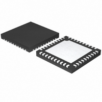
ISL97653AIRZ-TK Intersil, ISL97653AIRZ-TK Datasheet - Page 16

ISL97653AIRZ-TK
Manufacturer Part Number
ISL97653AIRZ-TK
Description
IC LCD SUPPLY 5CHN 40-QFN
Manufacturer
Intersil
Datasheet
1.ISL97653AIRZ.pdf
(18 pages)
Specifications of ISL97653AIRZ-TK
Applications
LCD TV/Monitor
Current - Supply
4mA
Voltage - Supply
4 V ~ 14 V
Operating Temperature
-40°C ~ 105°C
Mounting Type
Surface Mount
Package / Case
40-QFN
Lead Free Status / RoHS Status
Lead free / RoHS Compliant
V
The V
switching the voltage on COM between ground, DRN and
POUT, under control of the start-up sequence and the CTL pin.
During the start-up sequence, COM is pulled to ground via
an NDMOS FET with r
sequence has completed, CTL is enabled and acts as a
multiplexer control such that if CTL is low, COM connects to
DRN through a 30Ω internal MOSFET, and if CTL is high,
COM connects to P
The slew rate of the switch control circuit is mainly restricted
by the load capacitance at COM pin and is given by
Equation 20:
Where V
P
between COM and DRN or P
MOSFET r
inserted, R
C
In the Typical Application Circuit, R
bias to DRN based on Equation 21:
And R
ΔV
------- -
V
Δt
OUT
L
ON
DRN
is the load capacitance of switch control circuit.
=
, which range is from 0V to 30V. R
Slice Circuit
ON
------------------------------------ -
(
10
=
R
i
g
V
-------------------------------------------------------- -
can be adjusted to adjust the slew rate.
slice circuit functions as a three way multiplexer,
||
ON
is the supply voltage applied to DRN or voltage at
R
DS(on)
L
V
L
g
is the load resistance of VON slice circuit, and
) C
⋅
FAULT
×
R
R
9
9
, the trace resistance and the resistor
+AVDD R
L
+
1.2MHz
OUT
R
8
DS(ON)
A2
CLK
EN
internally via a 5Ω MOSFET.
⋅
8
16
OUT
0.4V
of 260Ω. After the start-up
STOP
CONTROL
including the internal
PWM
8
, R
A1
FIGURE 17. NEGATIVE CHARGE PUMP BLOCK DIAGRAM
VDD
9
i
is the resistance
and C
0.2V
22
give the
(EQ. 20)
(EQ. 21)
ISL97653A
M2
M1
SUPN
PGND
NOUT
FBN
820pF
V
An LDO controller is also integrated to provide a second
logic supply. The LDO-CTL pin drives the base of an
external transistor which should be sized for the current
required. A resistor divider is used to set the output voltage
by feeding back a reference voltage to LDO-FB. The internal
feedback reference is 1.215V.
HVS Operation
When the HVS input is taken high, the ISL97653A enters
HVS test mode. In this mode, the output of A
increased by switching RSET to ground, and the AVDD is
set to:
Where R
voltage higher than the maximum rating of the boost
MOSFET may damage the part.
Fault Protection
The ISL97653A incorporates a number of fault protection
schemes. AVDD, VON, and VOFF are constantly monitored.
If fault conditions are detected for longer than 1ms on these
FB inputs, the device stops switching and the outputs are
disconnected. The ISL97653A also integrates over-temp
and over current protection.
Supply Sequencing
When the input voltage V
V
fixed soft-start at start-up. A
dependant on the EN pin.
A
LOGIC,
LOGIC2
VDD
C20
220nF
C12
=
V
REF
R
-------------------- -
x
and V
3
is the value of R
LDO
R
+
R6
40k
x
R
LOGIC2
x
×
D3
V
FBB
100pF
328k
C19
are turned on. V
R7
D2
IN
4
VDD
is higher than 4V(UVLO), V
in parallel with R
, V
ON
C13
470nF
, and V
V
LOGIC
OFF
(-8V)
VDD
OFF
5
has a 9ms
. AVDD
September 7, 2010
is
are
(EQ. 22)
FN6367.3
REF
,


