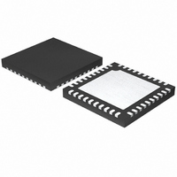
ISL97653AIRZ-TK Intersil, ISL97653AIRZ-TK Datasheet - Page 9

ISL97653AIRZ-TK
Manufacturer Part Number
ISL97653AIRZ-TK
Description
IC LCD SUPPLY 5CHN 40-QFN
Manufacturer
Intersil
Datasheet
1.ISL97653AIRZ.pdf
(18 pages)
Specifications of ISL97653AIRZ-TK
Applications
LCD TV/Monitor
Current - Supply
4mA
Voltage - Supply
4 V ~ 14 V
Operating Temperature
-40°C ~ 105°C
Mounting Type
Surface Mount
Package / Case
40-QFN
Lead Free Status / RoHS Status
Lead free / RoHS Compliant
Typical Performance Curves
Pin Descriptions
PIN NUMBER
3, 4
5, 6
10
12
13
14
15
16
17
18
19
20
21
22
23
24
11
1
2
7
8
9
FIGURE 13. BOOST CURRENT LIMIT
Ch1 = LXL (400ns/DIV)
Ch2 = ILXL (400ns/DIV)
PGND3, PGND4
LXL1, LXL2
PIN NAME
PGND5
PVIN2
NOUT
VREF
SUPN
SUPP
POUT
COM
CM2
DRN
FBN
C1P
C1N
C2P
C2N
FBP
FBL
CTL
CB
VL
9
Logic buck supply voltage. This is also the analog supply from which the VL is generated. Needs at
least 1µF bypassing.
Logic buck boot strap pin. Generate the gate drive voltage for the N-Channel MOSFET by connecting
a 1µF cap to the switching node LXL1, 2.
Logic buck switching node. Source of the high side internal power N-Channel MOSFET for the Buck.
Logic buck ground pin.
Buck compensation pin. An RC network is recommended. Increase R for better transient response at
the expense of stability.
Logic buck feedback pin. High impedance input to regulate at 1.215V.
5.25V internal regulator output. Bypass with a 4.7µF capacitor. Ref voltage is generated from VL.
Reference voltage output. Bypass with a low valued capacitor for transients - recommend 220nF.
Should not be greater than 5 times CDEL capacitor to ensure correct start-up sequence.
Negative charge pump feedback pin. High impedance input to regulate to 0.203V.
Negative charge pump supply voltage. Can be the same as or different from A
Negative charge pump driver output.
Charge pump ground pin.
Charge pump capacitor 1, positive connection.
Charge pump capacitor 1, negative connection.
Charge pump capacitor 2, positive connection.
Charge pump capacitor 2, negative connection.
Positive charge pump supply. Can be the same as or different from A
Positive charge pump feedback pin. High impedance input to regulate at 1.215V
V
High voltage switch control output. V
Lower reference voltage for V
Input control pin for V
ON
(Continued)
charge pump output.
ISL97653A
ON
slice output.
ON
slice output. Usually connected to A
ON
slice output.
DESCRIPTION
FIGURE 14. BUCK CURRENT LIMIT
Ch1 = LXL (400ns/DIV)
Ch2 = ILXL (400ns/DIV)
VDD.
VDD
.
VDD.
September 7, 2010
FN6367.3


