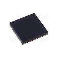
MAX15048ETJ+ Maxim Integrated Products, MAX15048ETJ+ Datasheet - Page 11

MAX15048ETJ+
Manufacturer Part Number
MAX15048ETJ+
Description
IC CTRLR PWM STP-DN TRIPL 32WQFN
Manufacturer
Maxim Integrated Products
Datasheet
1.MAX15048ETJ.pdf
(31 pages)
Specifications of MAX15048ETJ+
Applications
Power Supply Controller, Sequencer
Voltage - Supply
4.7 V ~ 23 V
Current - Supply
6mA
Operating Temperature
-40°C ~ 85°C
Mounting Type
Surface Mount
Package / Case
32-WQFN Exposed Pad
Number Of Outputs
3
Output Voltage
5 V
Input Voltage
4.7 V to 23 V
Supply Current
6 mA
Switching Frequency
200 KHz
Mounting Style
SMD/SMT
Maximum Operating Temperature
+ 85 C
Minimum Operating Temperature
- 40 C
Lead Free Status / RoHS Status
Lead free / RoHS Compliant
Voltage - Input
-
Lead Free Status / Rohs Status
Lead free / RoHS Compliant
PIN
12
13
14
15
16
17
18
19
20
21
22
23
24
25
26
27
28
29
30
31
32
—
PGOOD
COMP1
COMP3
DREG1
PGND1
DREG3
PGND3
NAME
BST1
BST3
______________________________________________________________________________________
DH1
DH3
REG
FB1
EN1
DL1
FB3
EN3
DL3
LX1
LX3
EP
IN
Controller Power-Good Output. Pull up PGOOD with a resistor to a positive voltage below 5.5V.
For the MAX15048, PGOOD output releases when all three V
MAX15049, PGOOD output releases when all three controllers are out of prebias and all three V
voltages are above 0.55V.
Controller 1 Transconductance Error-Amplifier Output. Connect COMP1 to the compensation
feedback network of output 1.
Controller 1 Feedback Regulation Point. Connect to the center tap of a resistive voltage-divider from
the converter output to SGND to set the output voltage. The FB1 voltage regulates to 0.6V (typ).
Controller 1 Enable Input. For tracking (MAX15048), EN1 must be above 0.6V, V
controller to start outputs 1, 2, and 3. Controller 1 is the master. Use the master as the highest output
voltage in a coincident tracking configuration. For the MAX15049, EN1 must be above 0.6V for the
PWM controller to start output 1.
Controller 1 High-Side Gate-Driver Supply. Connect a 0.1FF ceramic capacitor from BST1 to LX1.
Controller 1 High-Side Gate-Driver Output. DH1 drives the gate of the high-side MOSFET.
Controller 1 High-Side MOSFET Source Connection/Synchronous MOSFET Drain Connection.
Connect the inductor and the negative side of the boost capacitor to LX1.
Controller 1 Low-Side Gate-Driver Supply. Connect externally to REG through a 1I to 4.7I resistor.
Connect a minimum of 0.22FF ceramic capacitor from DREG1 to PGND1.
Controller 1 Low-Side Gate-Driver Output. DL1 is the gate-driver output for the synchronous MOSFET.
Controller 1 Power Ground. Connect the input filter capacitor’s negative terminal, the source of the
synchronous MOSFET, and the output filter capacitor’s return to PGND1. Connect to SGND at a
single point near the input capacitor return terminal.
Controller 3 Transconductance Error-Amplifier Output. Connect COMP3 to the compensation
feedback network of output 3.
Controller 3 Feedback Regulation Point. Connect to the center tap of a resistive voltage-divider from
the converter output to SGND to set the output voltage. The FB3 voltage regulates to 0.6V (typ).
Controller 3 Enable/Tracking Input. See Figure 2. When tracking (MAX15048), connect the same
resistive voltage-divider used for FB3 from output 1 to EN3 to SGND for coincident tracking. Connect
EN3 to analog ground for ratiometric tracking. When sequencing (MAX15049), EN3 must be above
0.6V for PWM controller 3 to start.
Controller 3 High-Side Gate-Driver Supply. Connect a 0.1FF ceramic capacitor from BST3 to LX3.
Controller 3 High-Side Gate-Driver Output. DH3 drives the gate of the high-side MOSFET.
Controller 3 High-Side MOSFET Source Connection/Synchronous MOSFET Drain Connection.
Connect the inductor and the negative side of the boost capacitor to LX3.
Controller 3 Low-Side Gate-Driver Supply. Connect externally to REG through a 1I to 4.7I resistor.
Connect a minimum of 0.22FF ceramic capacitor from DREG3 to PGND3.
Controller 3 Low-Side Gate-Driver Output. DL3 is the gate-driver output for the synchronous MOSFET.
Controller 3 Power Ground. Connect the input filter capacitor’s negative terminal, the source of the
synchronous MOSFET, and the output filter capacitor’s return to PGND3.
Supply Input Connection. Connect to an external voltage source from 4.7V to 23V. For 4.5V to 5.5V
input applications, connect IN and REG together.
5V Regulator Output. Bypass with a 2.2FF ceramic capacitor to SGND.
Exposed Pad. Solder the exposed pad to a large SGND plane to improve thermal dissipation.
Triple-Output Buck Controllers
with Tracking/Sequencing
FUNCTION
Pin Description (continued)
FB_
voltages are above 0.55V. For the
EN-TH
, for the PWM
FB_
11


