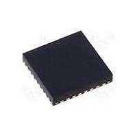
MAX15048ETJ+ Maxim Integrated Products, MAX15048ETJ+ Datasheet - Page 20

MAX15048ETJ+
Manufacturer Part Number
MAX15048ETJ+
Description
IC CTRLR PWM STP-DN TRIPL 32WQFN
Manufacturer
Maxim Integrated Products
Datasheet
1.MAX15048ETJ.pdf
(31 pages)
Specifications of MAX15048ETJ+
Applications
Power Supply Controller, Sequencer
Voltage - Supply
4.7 V ~ 23 V
Current - Supply
6mA
Operating Temperature
-40°C ~ 85°C
Mounting Type
Surface Mount
Package / Case
32-WQFN Exposed Pad
Number Of Outputs
3
Output Voltage
5 V
Input Voltage
4.7 V to 23 V
Supply Current
6 mA
Switching Frequency
200 KHz
Mounting Style
SMD/SMT
Maximum Operating Temperature
+ 85 C
Minimum Operating Temperature
- 40 C
Lead Free Status / RoHS Status
Lead free / RoHS Compliant
Voltage - Input
-
Lead Free Status / Rohs Status
Lead free / RoHS Compliant
Triple-Output Buck Controllers
with Tracking/Sequencing
(f
(see the Setting the Switching Frequency section). The
peak-to-peak inductor current (DI
the peak-to-peak output ripple, is worst at the maximum
input voltage. See the Output-Capacitor Selection sec-
tion to verify that the worst-case output current ripple is
acceptable. The inductor saturation current (I
important to avoid runaway current during continuous
output short-circuit conditions. Select an inductor with an
I
rent. Inductor parasitic resistance (DCR) causes copper
losses and affects efficiency. Select a low-loss inductor
having the lowest possible DCR that fits in the allocated
dimensions.
The discontinuous input current of the buck converter
causes large input-ripple currents, and therefore, the
input capacitor must be carefully chosen to withstand
the input-ripple current and keep the input-voltage
ripple within design requirements. The 120° ripple phase
operation increases the frequency of the input capacitor
ripple current to thrice the individual converter switching
frequency. When using ripple phasing, the worst-case
input-capacitor ripple current is when only one converter
with the highest output current is on.
The input-voltage ripple comprises DV
capacitor discharge) and DV
the input capacitor). The total voltage ripple is the sum of
DV
Calculate the input capacitance and ESR required for a
specified ripple using the following equations:
I
peak-to-peak inductor current, and f
frequency.
20
SAT
LOAD(MAX)
SW
Q
) is programmable between 200kHz and 1.2MHz
_____________________________________________________________________________________
and DV
specification higher than the maximum peak cur-
ESR
is the maximum output current, DI
∆
C
ESR
I
P-P
IN
, which peaks at the end of the on cycle.
=
=
=
I
LOAD(MAX)
(
I
V
LOAD(MAX)
IN
Input-Capacitor Selection
where:
(
- V
V
∆
IN
V
OUT_
∆
Q
ESR
V
×
ESR
+
f
×
SW
f
SW
)
(caused by the ESR of
+
V
×
×
∆
P-P
OUT_
V
V
)
SW
I
L
IN
OUT_
P-P
2
Q
), which reflects
is the switching
(caused by the
SAT
P-P
) is also
is the
For the condition with only one converter on, calculate
the input-ripple current using the following equation:
The MAX15048/MAX15049 include UVLO hysteresis to
avoid possible unintentional chattering during turn-on.
Use additional bulk capacitance if the input source
impedance is high. At lower input voltage, additional
input capacitance helps avoid possible undershoot
below the UVLO threshold during transient loading.
The allowed output-voltage ripple and the maximum
deviation of the output voltage during load steps deter-
mine the required output capacitance and its ESR. The
steady-state output ripple is mainly composed of DV
(caused by the capacitor discharge) and DV
by the voltage drop across the ESR of the output capaci-
tor). The equations for calculating the output capaci-
tance and its ESR are:
DV
out of phase from each other. If using ceramic capaci-
tors, which generally have low ESR, DV
using electrolytic capacitors, DV
The allowable deviation of the output voltage during fast-
load transients also affects the output capacitance, its
ESR, and its ESL. The output capacitor supplies the load
current during a load step until the controller responds
with a greater duty cycle. The response time (t
depends on the gain bandwidth of the converter (see the
Compensation Design Guidelines section). The resistive
drop across the output capacitor’s ESR, the drop across
the capacitor’s ESL, and the capacitor discharge causes
a voltage droop during the load-step (I
bination of low-ESR tantalum/aluminum electrolytic and
ceramic capacitors for better load-transient and voltage-
ripple performance. Nonleaded capacitors and capaci-
tors in parallel help reduce the ESL. Keep the maximum
output-voltage deviation below the tolerable limits of the
electronics being powered.
ESR
I
CIN(RMS)
and DV
=
Q
I
LOAD(MAX)
C
are not directly additive since they are
OUT
Output-Capacitor Selection
ESR
=
8
=
× ∆
×
∆
∆
V
∆
V
I
V
ESR
P-P
I
Q
OUT_
P-P
ESR
×
f
SW
dominates.
×
STEP
(
V
V
IN
Q
IN
). Use a com-
dominates. If
- V
ESR
RESPONSE
OUT_
(caused
)
Q
)


