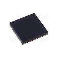
MAX15048ETJ+ Maxim Integrated Products, MAX15048ETJ+ Datasheet - Page 25

MAX15048ETJ+
Manufacturer Part Number
MAX15048ETJ+
Description
IC CTRLR PWM STP-DN TRIPL 32WQFN
Manufacturer
Maxim Integrated Products
Datasheet
1.MAX15048ETJ.pdf
(31 pages)
Specifications of MAX15048ETJ+
Applications
Power Supply Controller, Sequencer
Voltage - Supply
4.7 V ~ 23 V
Current - Supply
6mA
Operating Temperature
-40°C ~ 85°C
Mounting Type
Surface Mount
Package / Case
32-WQFN Exposed Pad
Number Of Outputs
3
Output Voltage
5 V
Input Voltage
4.7 V to 23 V
Supply Current
6 mA
Switching Frequency
200 KHz
Mounting Style
SMD/SMT
Maximum Operating Temperature
+ 85 C
Minimum Operating Temperature
- 40 C
Lead Free Status / RoHS Status
Lead free / RoHS Compliant
Voltage - Input
-
Lead Free Status / Rohs Status
Lead free / RoHS Compliant
Design procedures for both Type II and Type III compen-
sators are shown below.
Type II: Compensation when f
When the f
a Type II compensation network provides the neces-
sary closed-loop response. The Type II compensation
network provides a midband compensating zero and
high-frequency pole (see Figures 5a and 5b).
R
provides the high-frequency pole. Use the following proce-
dure to calculate the compensation network components:
1) Calculate the f
Figure 5a. Type II Compensation Network
Figure 5b. Type II Compensation Network Response
F
GAIN
(dB)
C
F
(AT ORIGIN)
provides the midband zero f
1ST POLE
G
MOD
2ND ASYMPTOTE
V
REF
ZERO, ESR
f
ZERO, ESR
V
OUT_ -1
R
R
1
2
1ST ZERO
V
(R
f
OUT_
LC
RF
F
______________________________________________________________________________________
ZERO, ESR
C
1ST ASYMPTOTE
G
F
)
MOD
V
-1
REF
=
is lower than f
V
REF
=
2
π ×
V
G
OUT_ -1
g
2
MOD
M
π ×
C
R
and LC double pole, f
F
V
L C
F
(ωC
REF
1
×
ESR C
CO
3RD ASYMPTOTE
V
F
OUT_ -1
)
MID, ZERO
-1
OUT
1
> f
CO
×
COMP_
(ωC
ZERO, ESR
C
and close to f
CF
CF
OUT
)
2ND POLE
-1
(R
Triple-Output Buck Controllers
F
C
, and R
CF
)
-1
ω(rad/s)
LC
F
C
LC
with Tracking/Sequencing
:
CF
,
2) Select the unity-gain crossover frequency as:
3) Determine R
Note: R
over frequency to unity, e.g., G
= 1V/V. The transconductance error-amplifier gain is
G
The total loop gain can be expressed logarithmically as
follows:
where V
to 1.2V:
4) Place a zero at or below the LC double pole, f
5) Place a high-frequency pole at or below f
6) Choose an appropriately sized R
where V
20 log
E/A
×
OUT_ to FB_, start with a 10kI). Once R
calculate R
(f
G
CO
10
MOD CO
F
[
RAMP
FB_
g R
) = g
is derived by setting the total loop gain at cross-
M F
R
(f
= 0.6V.
F
]
MOD
+
is the peak-to-peak ramp amplitude equal
2
=
20 log
F
)
using the following equation:
R
×
C
from the following:
=
V
C
2
RAMP
x R
CF
V
F
=
V
FB_
10
R
RAMP
f
V
=
CO
F
1
=
IN
, while the modulator gain is:
(2
×
×
2
(2
× π ×
V
π ×
π ×
V
≤
OUT_
π ×
IN
×
f
10
R
SW
R
f
2
CO
V
×
ESR V
f
1
F
π ×
F
FB_
CO
g
1
×
×
×
- V
E/A
MOD
ESR
×
L) V
f
f
f
SW
×
CO
LC
FB_
×
IN
(f
L) V
1
CO
×
×
OUT_
×
(connected from
V
L
ESR
OUT_
FB_
) x G
×
×
P
1
V
V
V
OUT_
is selected,
= 0.5 x f
RAMP
FB_
MOD
LC
(f
=
CO
0dB
:
SW
25
)
:


