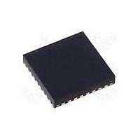
MAX15048ETJ+ Maxim Integrated Products, MAX15048ETJ+ Datasheet - Page 16

MAX15048ETJ+
Manufacturer Part Number
MAX15048ETJ+
Description
IC CTRLR PWM STP-DN TRIPL 32WQFN
Manufacturer
Maxim Integrated Products
Datasheet
1.MAX15048ETJ.pdf
(31 pages)
Specifications of MAX15048ETJ+
Applications
Power Supply Controller, Sequencer
Voltage - Supply
4.7 V ~ 23 V
Current - Supply
6mA
Operating Temperature
-40°C ~ 85°C
Mounting Type
Surface Mount
Package / Case
32-WQFN Exposed Pad
Number Of Outputs
3
Output Voltage
5 V
Input Voltage
4.7 V to 23 V
Supply Current
6 mA
Switching Frequency
200 KHz
Mounting Style
SMD/SMT
Maximum Operating Temperature
+ 85 C
Minimum Operating Temperature
- 40 C
Lead Free Status / RoHS Status
Lead free / RoHS Compliant
Voltage - Input
-
Lead Free Status / Rohs Status
Lead free / RoHS Compliant
Triple-Output Buck Controllers
with Tracking/Sequencing
The MAX15048/MAX15049 are triple-output, PWM, step-
down, DC-DC controllers with tracking and sequencing
options. The devices operate over the 4.7V to 23V or 5V
Q10% input voltage range. Each PWM controller pro-
vides an adjustable output down to 0.6V and delivers up
to 15A of load current with excellent load and line regu-
lation. The MAX15049 can start into prebiased outputs.
This ensures the glitch-free output voltage power-up in
the case of parallel power modules. The MAX15048/
MAX15049 are optimized for high performance, small-
size power-management solutions.
Each of the MAX15048/MAX15049 PWM sections utilizes
a voltage-mode control scheme for good noise immunity
and offer external compensation, allowing for maximum
flexibility with a wide selection of inductor values and
capacitor types. The devices operate at a fixed switching
frequency that is programmable from 200kHz to 1.2MHz.
Each converter, operating at up to 1.2MHz with 120° out-
of-phase, increases the input capacitor ripple frequency
up to 3.6MHz, reducing the RMS input-ripple current
and the size of the input bypass capacitor requirement
significantly.
The MAX15048 provides either coincident tracking
or ratiometric tracking, and the MAX15049 provides
sequencing. This allows tailoring of the power-up/power-
down sequence depending on the system requirements.
The MAX15048/MAX15049 integrate boost diodes for
additional system cost savings.
The MAX15048/MAX15049 feature lossless valley-mode
current-limit protection through monitoring the voltage
drop across the synchronous MOSFET’s on-resistance.
The internal current source of these devices exhibits a
positive temperature coefficient to help compensate for
the MOSFET’s temperature coefficient.
The MAX15048/MAX15049 include internal UVLO with
hysteresis, digital soft-start, and soft-stop (the MAX15048
only) for glitch-free power-up and power-down of the
converter. The power-good circuitry (PGOOD) monitors
all three outputs and provides a PGOOD signal to a
system controller/processor indicating when all outputs
are within regulation. Protection features include lossless
valley-mode current limit, hiccup mode output short-
circuit protection, and thermal shutdown.
V
operation can commence. The UVLO circuitry keeps the
16
IN
must exceed the default UVLO threshold before any
_____________________________________________________________________________________
Internal Undervoltage Lockout (UVLO)
Detailed Description
MOSFET drivers, oscillator, and all the internal circuitry
shut down to reduce current consumption. The UVLO
rising threshold is 4.2V with 300mV hysteresis.
The soft-start feature of the MAX15048/MAX15049 allows
the load voltage to ramp up in a controlled manner, elimi-
nating output-voltage overshoot. Soft-start begins after
V
is above 0.6V. The soft-start circuitry gradually ramps up
the reference voltage. This controls the rate of rise of the
output voltage and reduces input surge currents during
startup. The soft-start duration is 2048 clock cycles. The
output voltage is incremented through 64 equal steps.
The output reaches regulation when soft-start is com-
pleted, regardless of output capacitance and load.
For the MAX15048, soft-stop commences when the
enable input falls below 0.55V. The soft-stop circuitry
ramps down the reference voltage controlling the output
voltage rate of fall. The output voltage is decremented
through 64 equal steps in 2048 clock cycles.
The MAX15049 can start into a prebiased load. During
soft-start, both switches are kept off until the PWM com-
parator commands the first PWM pulse. Until then, the
converters do not sink current from the outputs. The first
PWM pulse occurs when the ramping reference voltage
increases above the FB_ voltage.
REG is the output terminal of a 5V LDO powered from
IN, which provides power to the IC. Connect REG
externally to DREG_ to provide power for the low-side
MOSFET gate drivers. Bypass REG to SGND with a
minimum 2.2FF ceramic capacitor. Place the capacitor
physically close to the MAX15048/MAX15049 to provide
good bypassing. REG is intended for powering only
the internal circuitry and should not be used to supply
power to external loads. REG can source up to 60mA.
This current, I
gate-drive current (I
where Q
of each of the respective high- and low-side external
MOSFETs at V
of the converter, and I
device at the switching frequency.
IN
Digital Soft-Start (MAX15048/MAX15049)/
exceeds the UVLO threshold and the enable input
I
GHS_
REG
REG
= I
GATE
and Q
Internal Linear Regulator (REG)
Q
Prebiased Output (MAX15049)
, includes quiescent current (I
+ [f
DREG_
= 5V, f
GLS _
SW
Q
is the quiescent current of the
OC(Q
):
SW
Soft-Stop (MAX15048)/
equal the total gate charge
is the switching frequency
GHS_
+ Q
GLS_
)]
Q
) and


