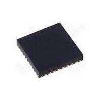
MAX15048ETJ+ Maxim Integrated Products, MAX15048ETJ+ Datasheet - Page 19

MAX15048ETJ+
Manufacturer Part Number
MAX15048ETJ+
Description
IC CTRLR PWM STP-DN TRIPL 32WQFN
Manufacturer
Maxim Integrated Products
Datasheet
1.MAX15048ETJ.pdf
(31 pages)
Specifications of MAX15048ETJ+
Applications
Power Supply Controller, Sequencer
Voltage - Supply
4.7 V ~ 23 V
Current - Supply
6mA
Operating Temperature
-40°C ~ 85°C
Mounting Type
Surface Mount
Package / Case
32-WQFN Exposed Pad
Number Of Outputs
3
Output Voltage
5 V
Input Voltage
4.7 V to 23 V
Supply Current
6 mA
Switching Frequency
200 KHz
Mounting Style
SMD/SMT
Maximum Operating Temperature
+ 85 C
Minimum Operating Temperature
- 40 C
Lead Free Status / RoHS Status
Lead free / RoHS Compliant
Voltage - Input
-
Lead Free Status / Rohs Status
Lead free / RoHS Compliant
Figure 3. Hiccup-Mode Block Diagram
just before the beginning of a new PWM cycle, the con-
troller skips that cycle. During severe overload or short-
circuit conditions, the switching frequency of the device
appears to decrease because the on-time of the low-side
MOSFET extends beyond a clock cycle.
If the current-limit threshold is exceeded for more than
eight cumulative clock cycles (N
down (both DH_ and DL_ are pulled low) for 4096 clock
cycles (hiccup timeout) and then restarts with a soft-
start sequence. If three consecutive cycles pass without
a current-limit event, the count of N
Figure 3). Hiccup mode protects the circuit against a
continuous output short circuit.
The MAX15048/MAX15049 feature an integrated ther-
mal-overload protection with temperature hysteresis.
Thermal-overload protection limits the total power dis-
sipation in the device and protects it in the event of an
extended thermal-fault condition. When the die tempera-
ture exceeds +160NC (typ), an internal thermal sensor
shuts down the device, turning off the power MOSFETs
and allowing the die to cool. After the die temperature
falls by +20NC (typ), the part restarts with a soft-start
sequence.
Connect a 15.625kI to 93.75kI resistor from RT to
SGND to program the switching frequency from 200kHz
to 1.2MHz. Calculate the switching frequency using the
following equation:
Higher switching frequencies allow designs with
lower inductor values and less output capacitance.
CURRENT LIMIT
f
Setting the Switching Frequency
SW
______________________________________________________________________________________
(kHz) = 12.8 O R
Thermal-Overload Protection
IN
CLR
IN
CLR
COUNT OF 8
COUNT OF 3
N
N
CLR
Design Procedure
CL
CL
RT
), the device shuts
CL
(kI)
is cleared (see
Triple-Output Buck Controllers
INITIATE HICCUP
TIMEOUT
N
HT
with Tracking/Sequencing
Consequently, peak currents and I
at higher switching frequencies, but core losses, gate-
charge currents, and switching losses increase.
Although the MAX15048/MAX15049 converters can
operate from input supplies ranging from 4.7V to 23V,
the input voltage range can be effectively limited by the
duty-cycle limitations for a given output voltage. The
maximum input voltage is limited by the minimum on-
time (t
where t
The minimum input voltage is limited by the maximum
duty cycle and is calculated using the following equa-
tion:
where t
Three key inductor parameters must be specified for
operation with the MAX15048/MAX15049: inductance
value (L), inductor saturation current (I
tor series resistance (DCR). The minimum required
inductance is a function of operating frequency, input-to-
output voltage differential, and the peak-to-peak inductor
current (DI
value. A lower inductance value minimizes size and
cost and improves large-signal and transient response.
However, efficiency is reduced due to higher peak cur-
rents and higher peak-to-peak output-voltage ripple for
the same output capacitor. A higher inductance increas-
es efficiency by reducing the ripple current; however,
resistive losses due to extra wire turns can exceed the
benefit gained from lower ripple current levels, especial-
ly when the inductance is increased without also allow-
ing for larger inductor dimensions. A good rule of thumb
is to choose DI
Calculate the inductance using the following equation:
V
optimum for typical conditions. The switching frequency
IN
and V
ON(MIN)
ON(MIN)
OFF(MIN)
P-P
OUT_
V
). Higher DI
):
L
IN(MIN)
V
P-P
IN(MAX)
is 75ns.
=
are typical values so that efficiency is
typically is equal to 300ns.
Effective Input Voltage Range
V
equal to 30% of the full load current.
OUT_
V
IN
=
1-(t
×
≤
(V
f
P-P
SW
t
ON(MIN)
OFF(MIN)
IN
allows for a lower inductor
- V
× ∆
V
V
OUT_
OUT_
OUT_
Inductor Selection
I
P-P
×
2
×
R losses are lower
f
)
SW
f
SW
SAT
)
), and induc-
19


