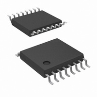
LM25037MT/NOPB National Semiconductor, LM25037MT/NOPB Datasheet - Page 11

LM25037MT/NOPB
Manufacturer Part Number
LM25037MT/NOPB
Description
IC CTLR PWM C/V MODE 16-TSSOP
Manufacturer
National Semiconductor
Series
PowerWise®r
Datasheet
1.LM25037MTNOPB.pdf
(24 pages)
Specifications of LM25037MT/NOPB
Pwm Type
Voltage/Current Mode
Number Of Outputs
1
Frequency - Max
578kHz
Duty Cycle
88%
Voltage - Supply
5.5 V ~ 75 V
Buck
No
Boost
No
Flyback
No
Inverting
No
Doubler
No
Divider
No
Cuk
No
Isolated
No
Operating Temperature
-40°C ~ 125°C
Package / Case
16-TSSOP
Frequency-max
578kHz
For Use With
LM25037EVAL - BOARD EVAL FOR LM25037
Lead Free Status / RoHS Status
Lead free / RoHS Compliant
Other names
LM25037MT
SOFT-START
The soft-start circuit allows the regulator to gradually reach a
steady state operating point, thereby reducing start-up stress-
es and current surges. When bias is supplied to the LM25037,
the SS pin capacitor is discharged by an internal MOSFET.
When the UVLO, VCC and REF pins reach their operating
thresholds, the SS capacitor is released and charged with a
100 µA current source. The PWM comparator control voltage
at the COMP pin is clamped to the SS pin voltage by an in-
ternal amplifier. When the PWM comparator input reaches
1V, output pulses commence with slowly increasing duty cy-
cle. The voltage at the SS pin eventually increases to 5V,
while the voltage at the PWM comparator increases to the
value required for regulation as determined by the voltage
feedback loop.
One method to disable the regulator is to ground the SS pin.
This forces the internal PWM control signal to ground, reduc-
ing the output duty cycle quickly to zero. Releasing the SS pin
initiates a soft-start sequence and normal operation resumes.
A second shutdown method is discussed in the UVLO section.
PWM COMPARATOR
The pulse width modulation (PWM) comparator compares the
voltage ramp signal at the RAMP pin to the loop error signal.
The loop error signal is derived from the internal error ampli-
fier (COMP pin). The resulting control voltage passes through
a 1V level shift before being applied to the PWM comparator.
This comparator is optimized for speed in order to achieve
minimum controllable duty cycles. The common mode input
voltage range of the PWM comparator is from 0 to 4.3V.
FIGURE 3. Current Limit Restart Timing
11
RAMP PIN
The voltage at the RAMP pin provides the modulation ramp
for the PWM comparator. The PWM comparator compares
the modulation ramp signal at the RAMP pin to the loop error
signal to control the output duty cycle. The modulation ramp
can be implemented either as a ramp proportional to input
voltage, known as feed-forward voltage mode control, or as
a ramp proportional to the primary current, known as current
mode control. The RAMP pin is reset by an internal FET with
an R
to configure the RAMP pin for either voltage mode or current
mode allows the controller to be implemented for the optimum
control method for the selected power stage topology. Con-
figuring RAMP pin is explained below and the differences
between voltage mode control and current mode control in
various double-ended topologies is explained in Applications
Information section.
FEED-FORWARD VOLTAGE MODE
An external resistor (R
VIN, AGND, and the RAMP pins is required to create the
PWM ramp signal as shown in
that the slope of the signal at RAMP will vary in proportion to
the input line voltage. This varying slope provides line feed-
forward information necessary to improve line transient re-
sponse with voltage mode control. The RAMP signal is
compared to the error signal by the pulse width modulator
comparator to control the duty cycle of the outputs. With a
constant error signal, the on-time (t
the input voltage (VIN) to stabilize the Volt • Second product
of the transformer primary. At the end of clock period, an in-
ternal FET will be enabled to reset the C
formulae for R
explained in Applications Information section. The amplitude
of the signal driving RAMP pin must not exceed the common
mode input voltage range of the PWM comparator (3.3V)
while in normal operation.
DS(ON)
of 5Ω (typical) at the end of every cycle. The ability
FF
and C
FF
FF
and component selection criteria are
) and capacitor (C
Figure 4
ON
) varies inversely with
below. It can be seen
FF
FF
) connected to
capacitor. The
30065120
www.national.com


