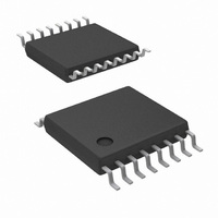
LM25037MT/NOPB National Semiconductor, LM25037MT/NOPB Datasheet - Page 5

LM25037MT/NOPB
Manufacturer Part Number
LM25037MT/NOPB
Description
IC CTLR PWM C/V MODE 16-TSSOP
Manufacturer
National Semiconductor
Series
PowerWise®r
Datasheet
1.LM25037MTNOPB.pdf
(24 pages)
Specifications of LM25037MT/NOPB
Pwm Type
Voltage/Current Mode
Number Of Outputs
1
Frequency - Max
578kHz
Duty Cycle
88%
Voltage - Supply
5.5 V ~ 75 V
Buck
No
Boost
No
Flyback
No
Inverting
No
Doubler
No
Divider
No
Cuk
No
Isolated
No
Operating Temperature
-40°C ~ 125°C
Package / Case
16-TSSOP
Frequency-max
578kHz
For Use With
LM25037EVAL - BOARD EVAL FOR LM25037
Lead Free Status / RoHS Status
Lead free / RoHS Compliant
Other names
LM25037MT
Oscillator (RT1 and RT2 Pins)
PWM Controller (Comp Pin)
Voltage Feed-Forward (RAMP Pin)
Error Amplifier
Main Output Drivers (OUTA and OUTB Pins)
Thermal Shutdown
Thermal Resistance
Note 1: Absolute Maximum Ratings are limits beyond which damage to the device may occur. Operating Ratings are conditions under which operation of the
device is intended to be functional. For guaranteed specifications and test conditions, see the Electrical Characteristics.
Note 2: COMP, RES are output pins. As such, it is not recommended that external power sources be connected to these pins.
Note 3: All limits are guaranteed. All electrical characteristics having room temperature limits are tested during production at T
are guaranteed by correlating the electrical characteristics to process and temperature variations and applying statistical process control.
Note 4: Typical specifications represent the most likely parametric norm at 25°C operation.
Note 5: The human body model is a 100 pF capacitor discharged through a 1.5 kΩ resistor into each pin. 2kV for all pins.
V
Symbol
PWM-OS
GBW
F
F
DT
DT
T
θ
θ
SW1
SW2
SD
JC
JA
1
2
Soft-Stop Current Sink
Dead-Time 1
Dead-Time 2
Frequency 1 (at OUTA, half
oscillator frequency)
Frequency 2 (at OUTA, half
oscillator frequency)
DC level
Input Sync threshold
Delay to output
SS to RAMP offset
Minimum duty cycle
COMP Open Circuit Voltage
COMP short circuit current
RAMP sink impedance(Clocked)
Gain Bandwidth
DC Gain
Input Voltage
COMP sink capability
FB Bias Current
Output high voltage
Output low voltage
Rise time
Fall time
Peak source current
Peak sink current
Thermal Shutdown Threshold
Thermal Shutdown Hysteresis
Junction to Case
Junction to Ambient
Parameter
V
R
R
R
R
R
R
V
V
V
V
V
I
I
C
C
V
V
TSSOP-16
TSSOP-16
OUT
OUT
SS
SS
FB
FB
FB
FB
VCC
VCC
RT2
RT2
RT1
RT2
RT1
RT2
LOAD
LOAD
= 0V
= 0V, COMP = 0V
= COMP
= 1.5V COMP=1V
= 2.0V
= 0V
= 50 mA, (Source)
= 100 mA (Sink)
= 15 kΩ
= 50 kΩ
= 30.1 kΩ,
= 30.1 kΩ,
= 11 kΩ,
= 30.1 kΩ,
= 10V
= 10V
= 1 nF
= 1 nF
5
Conditions
Vcc-0.5 Vcc-0.
1.22
Min
178
448
2.5
0.7
4.5
0.5
70
40
A
5
= 25°C. All hot and cold limits
1.245
4.75
Typ
100
250
200
515
165
125
0.2
1.2
1.2
75
65
75
13
10
25
17
18
25
29
2
3
1
1
5
4
www.national.com
Max
1.27
130
105
222
578
3.4
1.2
5.0
1.5
0.5
20
0
Units
°C/W
°C/W
MHz
kHz
kHz
mA
mA
µA
dB
nA
°C
°C
ns
ns
ns
ns
ns
%
Ω
V
V
V
V
V
V
V
A
A


