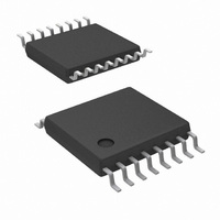
LM25037MT/NOPB National Semiconductor, LM25037MT/NOPB Datasheet - Page 3

LM25037MT/NOPB
Manufacturer Part Number
LM25037MT/NOPB
Description
IC CTLR PWM C/V MODE 16-TSSOP
Manufacturer
National Semiconductor
Series
PowerWise®r
Datasheet
1.LM25037MTNOPB.pdf
(24 pages)
Specifications of LM25037MT/NOPB
Pwm Type
Voltage/Current Mode
Number Of Outputs
1
Frequency - Max
578kHz
Duty Cycle
88%
Voltage - Supply
5.5 V ~ 75 V
Buck
No
Boost
No
Flyback
No
Inverting
No
Doubler
No
Divider
No
Cuk
No
Isolated
No
Operating Temperature
-40°C ~ 125°C
Package / Case
16-TSSOP
Frequency-max
578kHz
For Use With
LM25037EVAL - BOARD EVAL FOR LM25037
Lead Free Status / RoHS Status
Lead free / RoHS Compliant
Other names
LM25037MT
Pin
10
11
12
13
14
15
16
Pin Descriptions
1
2
3
4
5
6
7
8
9
COMP
RAMP
AGND
PGND
OUTB
OUTA
Name
UVLO
VCC
RES
REF
RT2
RT1
VIN
CS
FB
SS
Description
Pulse width modulator ramp
Line under-voltage lockout
Input to the pulse width modulator
Feedback
Oscillator dead-time control
Analog ground
Oscillator maximum on-time control
Current sense input
Restart timer
Soft-start
Power ground
Output driver
Output driver
Output of the high voltage start-up
regulator. The VCC voltage is
regulated to 7.7V.
Output of a 5V reference
Input voltage source
Application Information
Modulation ramp for the PWM comparator. This ramp can be a representative
of the primary current (current mode) or proportional to input voltage (feed-
forward voltage mode). This pin is reset to ground at the conclusion of every
cycle by an internal FET.
An external voltage divider from the power source sets the shutdown and
standby comparator threshold levels. When UVLO exceeds the 0.45V
shutdown threshold, the VCC and REF regulators are enabled. When UVLO
exceeds the 1.25V standby threshold, the SS pin is released and the device
enters the active mode.
Output of the error amplifier and input to the PWM comparator.
Connected to inverting input of the error amplifier. An internal 1.25V reference
is connected to the non-inverting input of the error amplifier. In isolated
applications using an external error amplifier, this pin should be connected to
the AGND pin.
The resistance connected between RT2 and AGND sets the forced dead-time
between switching periods of the alternating outputs.
Connect directly to Power Ground.
The resistance connected between RT1 and AGND sets the oscillator
maximum on-time. The sum of this maximum on-time and the forced dead-
time (set by RT2) sets the oscillator period.
If CS exceeds 250 mV the output pulse will be terminated, entering cycle-by-
cycle current limit. An internal switch holds CS low for 65 nS after either output
switches high to blank leading edge transients.
If cycle-by-cycle current limit is reached during any cycle, a 18 µA current is
sourced to the external RES pin capacitor. If the RES capacitor voltage
reaches 2.0V, the soft-start capacitor will be fully discharged and then
released with a pull-up current of 1 uA. After the first output pulse (when SS
= 1V), the SS pin charging current will increase to the normal level of 100 µA.
An external capacitor and an internal 100uA current source set the soft-start
ramp. The SS current source is reduced to 1 µA following a restart event (RES
pin high).
Connect directly to Analog Ground
Alternating gate drive output of the pulse width modulator. Capable of 1.2A
peak source and sink current.
Alternating gate drive output of the pulse width modulator. Capable of 1.2A
peak source and sink current.
If an auxiliary winding raises the voltage on this pin above the regulation set
point, the internal start-up regulator will shutdown thus reducing the IC power
dissipation. Locally decouple VCC with a 0.47 µF or greater capacitor.
Locally decouple with a 0.1 µF or greater capacitor. Maximum output current
is 10 mA (typ).
Input to the VCC Start-up regulator. Operating input range is 5.5V to 75V. For
power sources outside of this range, the LM25037 can be biased directly at
VCC by an external regulator.
3
www.national.com


