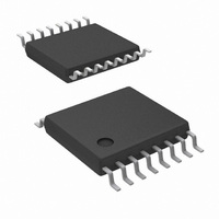
LM25037MT/NOPB National Semiconductor, LM25037MT/NOPB Datasheet - Page 15

LM25037MT/NOPB
Manufacturer Part Number
LM25037MT/NOPB
Description
IC CTLR PWM C/V MODE 16-TSSOP
Manufacturer
National Semiconductor
Series
PowerWise®r
Datasheet
1.LM25037MTNOPB.pdf
(24 pages)
Specifications of LM25037MT/NOPB
Pwm Type
Voltage/Current Mode
Number Of Outputs
1
Frequency - Max
578kHz
Duty Cycle
88%
Voltage - Supply
5.5 V ~ 75 V
Buck
No
Boost
No
Flyback
No
Inverting
No
Doubler
No
Divider
No
Cuk
No
Isolated
No
Operating Temperature
-40°C ~ 125°C
Package / Case
16-TSSOP
Frequency-max
578kHz
For Use With
LM25037EVAL - BOARD EVAL FOR LM25037
Lead Free Status / RoHS Status
Lead free / RoHS Compliant
Other names
LM25037MT
(VCC and REF) disabled. This helps to prevent catastrophic
failures from accidental device overheating. During thermal
shutdown, the soft-start capacitor is fully discharged and the
controller follows a normal start-up sequence after the junc-
tion temperature falls to the operating level (140°C).
Application Information
The following information is intended to provide guidelines for
the design process when applying the LM25037.
TOPOLOGY and CONTROL ALGORITHM CHOICE
The LM25037 has all the features required to implement dou-
ble-ended power converter topologies such as push-pull, half-
bridge and full-bridge with minimum external components.
One key feature is the flexibility in control algorithm selection,
i.e., the LM25037 can be used to implement either voltage
mode control or current mode control. Designers familiar with
these topologies recognize that conventionally, current mode
control is used for push-pull and full-bridge topologies while
voltage mode control is required for the half-bridge topology.
In limited applications, voltage mode control can be used for
push-pull and full-bridge topologies as well, with special care
to maintain flux balance, such as using a dc-blocking capac-
itor in the primary (full-bridge). The goal of this section is to
illustrate implementation of both current mode control and
voltage mode control using the LM25037 and aid the designer
in the design process.
VOLTAGE MODE CONTROL USING THE LM25037
An external resistor (R
VIN, AGND, and the RAMP pins is required to create a saw-
tooth modulation ramp signal shown in
the signal at RAMP will vary in proportion to the input line
voltage. The varying slope provides line feed-forward infor-
mation necessary to improve line transient response with
voltage mode control. With a constant error signal, the on-
time (t
stabilize the Volt • Second product of the transformer primary.
ON
) varies inversely with the input voltage (VIN) to
FF
) and capacitor (C
FIGURE 8. Feed-Forward Voltage Mode Configuration
Figure
FF
) connected to
8. The slope of
15
Using a line feed-forward ramp for PWM control requires very
little change in the voltage regulation loop to compensate for
changes in input voltage, as compared to a fixed slope oscil-
lator ramp. Furthermore, voltage mode control is less sus-
ceptible to noise and does not require leading edge filtering,
and is therefore a good choice for wide input range power
converters. Voltage mode control requires a more complicat-
ed compensation network, due to the complex-conjugate
poles of the L-C output filter.
In push-pull and full-bridge topologies, any asymmetry in the
volt-second product applied to primary in one phase may not
be cancelled by subsequent phase, possibly resulting in a dc
current build-up in the transformer, which pushes the trans-
former core towards saturation. Special care in the trans-
former design, such as gapping the core, or adding ballasting
resistance in the primary is required to rectify this imbalance
when using voltage mode control with these topologies. Cur-
rent mode control naturally corrects for any volt-second asym-
metry in the primary.
The recommended capacitor value range for C
1500 pF. Referring to
C
charged within the clock (CLK) pulse width each cycle. The
CLK pulse width is same as the dead-time set by RT2. The
minimum possible dead-time for LM25037 is 50 ns and the
internal discharge FET R
The value of R
For example, assuming a V
compromise of signal range and noise immunity), oscillator
frequency, F
pF results in a value for R
FF
must be small enough such that the capacitor can be dis-
OSC
FF
of 250 kHz, VIN
required can be calculated from
Figure
DS(ON)
FF
Ramp
of 348 kΩ.
8, it can be seen that value
is 5Ω (typical),
min
of 1 volt at VIN
of 24 Volts, and C
30065121
FF
www.national.com
is 100 pF to
min
FF
(a good
= 270


