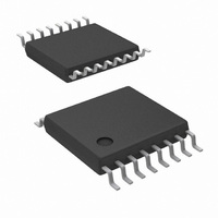
LM25037MT/NOPB National Semiconductor, LM25037MT/NOPB Datasheet - Page 21

LM25037MT/NOPB
Manufacturer Part Number
LM25037MT/NOPB
Description
IC CTLR PWM C/V MODE 16-TSSOP
Manufacturer
National Semiconductor
Series
PowerWise®r
Datasheet
1.LM25037MTNOPB.pdf
(24 pages)
Specifications of LM25037MT/NOPB
Pwm Type
Voltage/Current Mode
Number Of Outputs
1
Frequency - Max
578kHz
Duty Cycle
88%
Voltage - Supply
5.5 V ~ 75 V
Buck
No
Boost
No
Flyback
No
Inverting
No
Doubler
No
Divider
No
Cuk
No
Isolated
No
Operating Temperature
-40°C ~ 125°C
Package / Case
16-TSSOP
Frequency-max
578kHz
For Use With
LM25037EVAL - BOARD EVAL FOR LM25037
Lead Free Status / RoHS Status
Lead free / RoHS Compliant
Other names
LM25037MT
HICCUP MODE CURRENT LIMIT RESTART (RES)
The basic operation of the hiccup mode current limit is de-
scribed in the functional description. The delay time to the
In the case of continuous cycle-by-cycle current limit detec-
tion at the CS pin, the time required for C
hiccup mode threshold is:
For example, if C
2.0 ms. The cool down time, t2 is set by the soft-start capacitor
(C
to:
If C
The soft-start time t3 is set by the internal 100 µA current
source, and is equal to:
If C
The time t2 provides a periodic cool-down time for the power
converter in the event of a sustained overload or short circuit.
This off time results in lower average input current and lower
power dissipation within the power components. It is recom-
mended that the ratio of t2 / (t1 + t3) be in the range of 5 to
10 to take advantage of this feature.
If the application requires no delay from the first detection of
a current limit condition to the onset of the hiccup mode (t1 =
0), the RES pin can be left open (no external capacitor). If it
is desired to disable the hiccup mode entirely, the RES pin
should be connected to ground (AGND).
PRINTED CIRCUIT BOARD LAYOUT
The LM25037 Current Sense and PWM comparators are very
fast, and respond to short duration noise pulses. The compo-
nents at the CS, COMP, SS, UVLO, RT2 and the RT1 pins
SS
SS
SS
) and the internal 1 µA SS current source, and is equal
= 0.01 µF, t2 is
= 0.01 µF, t3 is
RES
= 0.01 µF the time t1 is approximately
≊
≊
10 ms.
400 µs.
FIGURE 16. Hiccup Over-Load Restart Timing
RES
to reach the 2.0V
21
initiation of a hiccup cycle is programmed by the selection of
the RES pin capacitor C
should be as physically close as possible to the IC, thereby
minimizing noise pickup on the PC board trace inductances.
Layout considerations are critical for the current sense filter.
If a current sense transformer is used, both leads of the trans-
former secondary should be routed to the sense filter com-
ponents and to the IC pins. The ground side of the transformer
should be connected via a dedicated PC board trace to the
AGND pin, rather than through the ground plane.
If the current sense circuit employs a sense resistor in the
drive transistor source, low inductance resistors should be
used. In this case, all the noise sensitive, low-current ground
trace should be connected in common near the IC, and then
a single connection made to the power ground (sense resistor
ground point).
While employing current mode control, RAMP pin capacitor
and CS pin capacitor must be placed close to the IC. Also, a
short direct trace should be employed to connect RAMP ca-
pacitor to the CS pin.
The gate drive outputs of the LM25037 should have short,
direct paths to the power MOSFETs in order to minimize in-
ductance in the PC board The two ground pins (AGND,
PGND) must be connected together with a short, direct con-
nection, to avoid jitter due to relative ground bounce.
If the internal dissipation of the LM25037 produces high junc-
tion temperatures during normal operation, the use of multiple
vias under the IC to a ground plane can help conduct heat
away from the IC. Judicious positioning of the PC board within
the end product, along with use of any available air flow
(forced or natural convection) will help reduce the junction
temperatures. If using forced air cooling, avoid placing the
LM25037 in the airflow shadow of tall components, such as
input capacitors.
APPLICATION EXAMPLE
The following schematic shows an example of a 50W push-
pull converter controlled by LM25037. The operating input
voltage range is 16V to 32V, and the output voltage is 5V. The
output current capability is 10 Amps. The converter is config-
ured for current mode control with external slope compensa-
tion. An auxiliary winding of the output filter inductor L3 is used
to raise the VCC voltage to reduce the power dissipation.
RES
as illustrated in
30065120
Figure
www.national.com
16.


