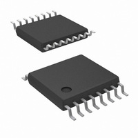
LM25037MT/NOPB National Semiconductor, LM25037MT/NOPB Datasheet - Page 17

LM25037MT/NOPB
Manufacturer Part Number
LM25037MT/NOPB
Description
IC CTLR PWM C/V MODE 16-TSSOP
Manufacturer
National Semiconductor
Series
PowerWise®r
Datasheet
1.LM25037MTNOPB.pdf
(24 pages)
Specifications of LM25037MT/NOPB
Pwm Type
Voltage/Current Mode
Number Of Outputs
1
Frequency - Max
578kHz
Duty Cycle
88%
Voltage - Supply
5.5 V ~ 75 V
Buck
No
Boost
No
Flyback
No
Inverting
No
Doubler
No
Divider
No
Cuk
No
Isolated
No
Operating Temperature
-40°C ~ 125°C
Package / Case
16-TSSOP
Frequency-max
578kHz
For Use With
LM25037EVAL - BOARD EVAL FOR LM25037
Lead Free Status / RoHS Status
Lead free / RoHS Compliant
Other names
LM25037MT
(F
current sense resistor (R
of 80 mV will suffice. The slope compensation "volts" that re-
sults from the above expression is the maximum voltage of
the artificial ramp added linearly to the RAMP pin till the end
of maximum switching period. For circuits where a current
sense tramsformer is used for primary current sensing, the
turns-ratio of the current sense transformer has to be taken
into account.
C
by the internal RAMP discharge FET. Capacitor values rang-
ing from 100 pF to 1500 pF are recommended. The value
must be small enough such that the capacitor can be dis-
charged within the clock (CLK) pulse width each cycle.
R
For example, with a C
erence voltage of 5V (V
and R
VIN and VCC
The voltage applied to the VIN pin, which may be the same
as the system voltage applied to the power transformer’s pri-
mary (V
current into the VIN pin depends primarily on the gate charge
provided by the output drivers, the switching frequency, and
any external loads on the VCC and REF pins. It is recom-
mended that the filter shown in
transients that may occur at the input supply. This is particu-
larly important when VIN is operated close to the maximum
operating rating of the LM25037.
When power is applied to VIN and the UVLO pin voltage is
greater than 0.45V, the VCC regulator is enabled and sup-
plies current into an external capacitor connected to the VCC
pin. When the voltage on the VCC pin reaches the regulation
point of 7.7V, the voltage reference (REF) is enabled. The
reference regulation set point is 5V. The outputs (OUTA and
OUTB) are enabled when the two bias regulators reach their
set point and the UVLO pin potential is greater than 1.25V. In
typical applications, an auxiliary transformer winding is con-
nected through a diode to the VCC pin. This winding must
raise the VCC voltage above 8.1V to shut off the internal start-
up regulator.
After the outputs are enabled and the external VCC supply
voltage has begun supplying power to the IC, the current into
the VIN pin drops below 1 mA. VIN should remain at a voltage
equal to or above the VCC voltage to avoid reverse current
through protection diodes.
slope
slope
OSC
) of 250 kHz, a filter inductance of 4 µH (L
filter
should be selected such that it can be fully discharged
can be selected from the following formula:
PWR
= 25Ω results in R
), can vary in the range from 5.5V to 75V. The
slope
REF
CS
of 1500 pF, F
) of 32 mΩ, slope compensation
), slope compensation of 80 mV
slope
Figure 10
value of 165 kΩ.
be used to suppress
OSC
of 250 kHz, ref-
Filter
) and a
17
FOR APPLICATIONS WITH >75V INPUT
For applications where the system input voltage exceeds 75V
or the IC power dissipation is of concern, the LM25037 can
be powered from an external start-up regulator as shown in
Figure
should be connected together. The voltage at the VCC and
VIN pins must be at least 5.5V (> Max VCC UV voltage) yet
not exceed 14V. An auxiliary winding can be used to reduce
the power dissipation in the external regulator once the power
converter is active. The NPN base-emitter reverses break-
down voltage, which can be as low as 5V for some transistors,
should be considered when selecting the transistor.
CURRENT SENSE
The CS pin should receive an input signal representative of
the transformer’s primary current, either from a current sense
transformer or from a resistor in series with the source of the
OUTA and OUTB MOSFET switches. In both cases, the
sensed current creates a voltage ramp across R1, and the
R
ure 12
close to the LM25037 as possible, and the ground connection
from the current sense transformer, or R1, should be a dedi-
cated track to the AGND pin. The current sense components
must provide greater than 220 mV at the CS pin when an over-
current condition exists.
F
/C
F
FIGURE 11. Start-up Regulator for VPWR >75V
filter suppresses noise and transients as shown in
11. In this configuration, the VIN and the VCC pins
and
FIGURE 10. Input Transient Protection
Figure
13. R1, R
F
and C
F
should be located as
30065134
www.national.com
Fig-
30065135


