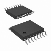
LM25037MT/NOPB National Semiconductor, LM25037MT/NOPB Datasheet - Page 14

LM25037MT/NOPB
Manufacturer Part Number
LM25037MT/NOPB
Description
IC CTLR PWM C/V MODE 16-TSSOP
Manufacturer
National Semiconductor
Series
PowerWise®r
Datasheet
1.LM25037MTNOPB.pdf
(24 pages)
Specifications of LM25037MT/NOPB
Pwm Type
Voltage/Current Mode
Number Of Outputs
1
Frequency - Max
578kHz
Duty Cycle
88%
Voltage - Supply
5.5 V ~ 75 V
Buck
No
Boost
No
Flyback
No
Inverting
No
Doubler
No
Divider
No
Cuk
No
Isolated
No
Operating Temperature
-40°C ~ 125°C
Package / Case
16-TSSOP
Frequency-max
578kHz
For Use With
LM25037EVAL - BOARD EVAL FOR LM25037
Lead Free Status / RoHS Status
Lead free / RoHS Compliant
Other names
LM25037MT
www.national.com
OSCILLATOR
The LM25037 oscillator frequency and the maximum duty cy-
cle are set by two external resistors connected between the
RT1 and RT2 pins to AGND. The minimum dead-time be-
tween OUTA and OUTB pulses is proportional to the RT2
resistor value and the overall oscillator frequency is inversely
proportional to RT1 and RT2 resistor values. Each output
switches at half the oscillator frequency. Initially, RT2 should
be selected for the desired dead-time or for the desired max-
imum duty cycle (D
As shown in
same as the dead-time set by RT2. This dead-time pulse is
used to limit the maximum duty cycle for each of the outputs.
Also, the discharge FET connected to the RAMP pin is en-
abled during the dead-time every clock period. The voltages
at both the RT1 and RT2 pins are internally regulated to a
nominal 2V. Both the resistors RT1 and RT2 should be locat-
ed as close as possible to the IC, and connected directly to
the pins. The tolerance of the external resistors and the fre-
quency tolerance indicated in the Electrical Characteristics
table must be taken into account when determining the worst
case frequency range.
SYNC CAPABILITY
The LM25037 can be synchronized to an external clock by
applying a narrow ac pulse to the RT1 pin. The external clock
must be at least 10% higher than the free-running oscillator
frequency set by the RT1 and RT2 resistors. If the external
clock frequency is less than the programmed frequency, the
LM25037 will ignore the synchronizing pulses. The synchro-
nization pulse width at the RT1 pin must be a minimum of 15
ns wide. The synchronization signal should be coupled into
the RT1 pin through a 100 pF capacitor or another value small
enough to ensure the sync pulse width at RT1 is less than
Figure
max
7, the internal clock pulse width is the
).
FIGURE 7. Timing Diagram of OUTA, OUTB and Dead-Time Set by RT2
14
It is recommended to set the dead-time range between 50 ns
and 250 ns. Beyond 250 ns, RT2 becomes excessively large,
and is prone to noise pickup. Fixed internal delays limit the
dead-time to greater than 50 ns. After the dead-time has been
programmed by RT2, the overall oscillator frequency can be
set by selecting resistor RT1 from :
For example, if the desired oscillator frequency is 400 kHz
(OUTA and OUTB each switching at 200 kHz) and desired
dead-time is 100 ns, the maximum duty cycle for each output
will be 96% and the values of RT1 and RT2 will be 15 kΩ and
20 kΩ respectively.
60% of the clock period under all conditions. When the syn-
chronizing pulse transitions from low-to-high (rising edge), the
voltage at the RT1 pin must be driven to exceed 3.0V from its
nominal 2.0V volt dc level. During the synchronization clock
signal’s low time, the voltage at the RT1 pin will be clamped
at 2V volts by an internal regulator. The RT1 and RT2 resis-
tors are always required, whether the oscillator is free running
or externally synchronized.
GATE DRIVER OUTPUTS (OUTA & OUTB)
The LM25037 provides two alternating gate driver outputs,
OUTA and OUTB. The internal gate drivers can each source
and sink 1.2A peak each. The maximum duty cycle is inher-
ently limited to less than 50% and is based on the value of
RT2 resistor. As an example, if the COMP pin is in a high
state, RT1 = 15K and RT2 = 20K then the outputs will operate
at maximum duty cycle of 96%.
THERMAL PROTECTION
Internal Thermal Shutdown circuitry is provided to protect the
integrated circuit in the event the maximum rated junction
temperature is exceeded. When activated, typically at 165°C,
the controller is forced into a low power standby state with the
output drivers (OUTA and OUTB) and the bias regulators
30065127


