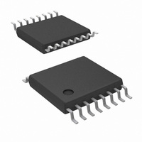
LM25037MT/NOPB National Semiconductor, LM25037MT/NOPB Datasheet - Page 4

LM25037MT/NOPB
Manufacturer Part Number
LM25037MT/NOPB
Description
IC CTLR PWM C/V MODE 16-TSSOP
Manufacturer
National Semiconductor
Series
PowerWise®r
Datasheet
1.LM25037MTNOPB.pdf
(24 pages)
Specifications of LM25037MT/NOPB
Pwm Type
Voltage/Current Mode
Number Of Outputs
1
Frequency - Max
578kHz
Duty Cycle
88%
Voltage - Supply
5.5 V ~ 75 V
Buck
No
Boost
No
Flyback
No
Inverting
No
Doubler
No
Divider
No
Cuk
No
Isolated
No
Operating Temperature
-40°C ~ 125°C
Package / Case
16-TSSOP
Frequency-max
578kHz
For Use With
LM25037EVAL - BOARD EVAL FOR LM25037
Lead Free Status / RoHS Status
Lead free / RoHS Compliant
Other names
LM25037MT
www.national.com
Startup Regulator (VCC Pin)
Voltage Reference Regulator (REF Pin)
Under-Voltage Lock Out and Shutdown (UVLO Pin)
Current Sense Input (CS Pin)
Current Limit Restart (RES Pin)
Soft-Start (SS Pin)
Absolute Maximum Ratings
If Military/Aerospace specified devices are required,
please contact the National Semiconductor Sales Office/
Distributors for availability and specifications.
VIN to GND
VCC, RAMP , OUTA, OUTB to GND
CS to GND
UVLO, FB, RT2, RT1, SS, REF to GND
COMP,
Electrical Characteristics
apply over full operating junction temperature range of −40°C to + 125°C. V
kΩ, V
Symbol
V
V
I
I
VCC(Lim)
REF(Lim)
V
VCC(UV)
V
REF(UV)
I
UVLO
V
V
UVLO
V
I
UVLO
I
VCC
VIN
RES
REF
SS
CS
RES(Note
= 3V unless otherwise stated. See Note
2)
VCC voltage
VCC current limit
VCC Under-voltage threshold
Hysteresis
Startup regulator current
Supply current into VCC from
external source
REF Voltage
REF Voltage Regulation
REF Current Limit
VREF Under-Voltage Threshold
Hysteresis
Under-voltage threshold
Hysteresis current
Under-voltage Shutdown
Threshold
Hysteresis
Current Limit Threshold
CS delay to output
Leading edge blanking time at CS
CS sink impedance (clocked)
RES Threshold
Charge source current
Discharge sink current
Charging current in normal
operation
Charging current during a hiccup
mode restart
Parameter
-0.3V to 76V
-0.3V to 16V
-0.3V to 1.0V
-0.3V to 7V
Specifications with standard typeface are for T
(Note
3(Note
1)
I
V
V
V
Outputs & COMP open, V
Outputs switching
I
I
V
UVLO pin sinking
UVLO voltage rising
CS from zero to 1V. Time for OUTA and
OUTB to fall to 90% of VCC. Output load
= 0 pF.
Internal FET sink impedance
V
V
V
V
VCC
REF
REF
VCC
VIN
VIN
REF
RES
RES
SS
SS
3) and Note
= 0
= 0
= 0 mA
= 0 to 2.5 mA
= 10 mA
= 20V, V
= 75V, V
= 4.5V
= 7V
= 1.5V
= 1V
4
VIN Voltage
External Voltage Applied to VCC
Operation Junction Temperature
ESD
Storage Temperature Range
Junction Temperature
Operating Ratings
UVLO
UVLO
Human Body Model
Conditions
4(Note
Rating(Note
= 0V
= 0V
VIN
4).
= 12V, V
VCC
= 10V,
5)
VCC
J
= 25°C, and those with boldface type
= 10V, R
4.75
1.20
0.35
0.22
Min
7.2
4.6
3.7
1.9
0.6
20
17
14
70
RT1
5
5
= 30.1 kΩ, R
0.255
1.25
0.45
Typ
100
7.7
0.5
0.4
0.1
35
45
10
22
27
65
21
18
−40°C to + 125°C
2kV
−65°C to + 150°C
150°C
5
4
5
7
4
2
8
1
1.295
5.5V to 75V
Max
5.15
0.29
130
8.1
5.4
4.3
0.6
2.2
1.4
58
80
25
26
45
21
11
8V to 14V
RT2
= 30.1
Units
mA
mA
mV
mA
µA
µA
µA
µA
µA
µA
µA
ns
ns
Ω
V
V
V
V
V
V
V
V
V
V
V


