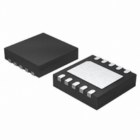
ISL6545ACRZ Intersil, ISL6545ACRZ Datasheet - Page 12

ISL6545ACRZ
Manufacturer Part Number
ISL6545ACRZ
Description
IC PWM BUCK BST VM 10DFN
Manufacturer
Intersil
Datasheet
1.ISL6545ACBZ-T.pdf
(16 pages)
Specifications of ISL6545ACRZ
Pwm Type
Voltage Mode
Number Of Outputs
1
Frequency - Max
660kHz
Duty Cycle
100%
Voltage - Supply
4.5 V ~ 14.4 V
Buck
Yes
Boost
Yes
Flyback
No
Inverting
No
Doubler
No
Divider
No
Cuk
No
Isolated
No
Operating Temperature
0°C ~ 70°C
Package / Case
10-DFN
Frequency-max
660kHz
Lead Free Status / RoHS Status
Lead free / RoHS Compliant
Figure 10 shows an asymptotic plot of the DC/DC converter’s
gain vs frequency. The actual Modulator Gain has a high gain
peak dependent on the quality factor (Q) of the output filter,
which is not shown. Using the above guidelines should yield a
compensation gain similar to the curve plotted. The open loop
error amplifier gain bounds the compensation gain. Check the
compensation gain at F
amplifier. The closed loop gain, G
log-log graph of Figure 10 by adding the modulator gain, G
(in dB), to the feedback compensation gain, G
equivalent to multiplying the modulator transfer function and the
compensation transfer function and then plotting the resulting
gain.
A stable control loop has a gain crossing with close to a
-20dB/decade slope and a phase margin greater than 45°.
Include worst case component variations when determining
phase margin. The mathematical model presented makes a
number of approximations and is generally not accurate at
frequencies approaching or exceeding half the switching
frequency. When designing compensation networks, select
target crossover frequencies in the range of 10% to 30% of
the switching frequency, F
This is just one method to calculate compensation
components; there are variations of Equations 3 through 9.
The error amp is similar to that on other Intersil regulators,
so existing tools can be used here as well. Special
consideration is needed if the size of a ceramic output
capacitance in parallel with bulk capacitors gets too large;
the calculation needs to model them both separately
(attempting to combine two different capacitors types into
one composite component model may not work properly; a
special tool may be needed; contact Intersil at
http://www.intersil.com/contacts/
Component Selection Guidelines
Output Capacitor Selection
An output capacitor is required to filter the output and supply
the load transient current. The filtering requirements are a
function of the switching frequency and the ripple current.
FIGURE 10. ASYMPTOTIC BODE PLOT OF CONVERTER GAIN
0
LOG
20
log
⎛
⎝
R2
------- -
R1
⎞
⎠
F
Z1
F
F
P2
LC
Z2
against the capabilities of the error
SW
F
F
12
CE
P1
.
CL
for assistance.
F
0
, is constructed on the
F
20
P2
log
G
CL
COMPENSATION GAIN
d
---------------------------------
OPEN LOOP E/A GAIN
CLOSED LOOP GAIN
MAX V
G
V
FB
MOD
MODULATOR GAIN
OSC
FREQUENCY
(in dB). This is
⋅
IN
ISL6545, ISL6545A
G
FB
MOD
The load transient requirements are a function of the slew
rate (di/dt) and the magnitude of the transient load current.
These requirements are generally met with a mix of
capacitors and careful layout.
Modern components and loads are capable of producing
transient load rates above 1A/ns. High frequency capacitors
initially supply the transient and slow the current load rate
seen by the bulk capacitors. The bulk filter capacitor values
are generally determined by the ESR (Effective Series
Resistance) and voltage rating requirements rather than
actual capacitance requirements.
High frequency decoupling capacitors should be placed as
close to the power pins of the load as physically possible. Be
careful not to add inductance in the circuit board wiring that
could cancel the usefulness of these low inductance
components. Consult with the manufacturer of the load on
specific decoupling requirements.
Use only specialized low-ESR capacitors intended for
switching-regulator applications for the bulk capacitors. The
bulk capacitor’s ESR will determine the output ripple voltage
and the initial voltage drop after a high slew-rate transient. An
aluminum electrolytic capacitor’s ESR value is related to the
case size with lower ESR available in larger case sizes.
However, the Equivalent Series Inductance (ESL) of these
capacitors increases with case size and can reduce the
usefulness of the capacitor to high slew-rate transient loading.
Unfortunately, ESL is not a specified parameter. Work with
your capacitor supplier and measure the capacitor’s
impedance with frequency to select a suitable component. In
most cases, multiple electrolytic capacitors of small case size
perform better than a single large case capacitor.
Output Inductor Selection
The output inductor is selected to meet the output voltage
ripple requirements and minimize the converter’s response
time to the load transient. The inductor value determines the
converter’s ripple current and the ripple voltage is a function
of the ripple current. The ripple voltage and current are
approximated by the equations shown in Equation 10:
Increasing the value of inductance reduces the ripple current
and voltage. However, the large inductance values reduce
the converter’s response time to a load transient.
One of the parameters limiting the converter’s response to
a load transient is the time required to change the inductor
current. Given a sufficiently fast control loop design, the
ISL6545x will provide either 0% or 100% duty cycle in
response to a load transient. The response time is the time
required to slew the inductor current from an initial current
value to the transient current level. During this interval the
difference between the inductor current and the transient
current level must be supplied by the output capacitor.
ΔI =
V
IN
Fsw x L
- V
OUT
x
V
V
OUT
IN
ΔV
OUT
= ΔI x ESR
March 3, 2011
(EQ. 10)
FN6305.6


