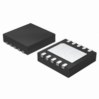
ISL6545ACRZ Intersil, ISL6545ACRZ Datasheet - Page 13

ISL6545ACRZ
Manufacturer Part Number
ISL6545ACRZ
Description
IC PWM BUCK BST VM 10DFN
Manufacturer
Intersil
Datasheet
1.ISL6545ACBZ-T.pdf
(16 pages)
Specifications of ISL6545ACRZ
Pwm Type
Voltage Mode
Number Of Outputs
1
Frequency - Max
660kHz
Duty Cycle
100%
Voltage - Supply
4.5 V ~ 14.4 V
Buck
Yes
Boost
Yes
Flyback
No
Inverting
No
Doubler
No
Divider
No
Cuk
No
Isolated
No
Operating Temperature
0°C ~ 70°C
Package / Case
10-DFN
Frequency-max
660kHz
Lead Free Status / RoHS Status
Lead free / RoHS Compliant
Minimizing the response time can minimize the output
capacitance required.
The response time to a transient is different for the
application of load and the removal of load. The equations in
Equation 11 give the approximate response time interval for
application and removal of a transient load:
where: I
response time to the application of load, and t
response time to the removal of load. The worst case
response time can be either at the application or removal of
load. Be sure to check both of these equations at the
minimum and maximum output levels for the worst case
response time.
Input Capacitor Selection
Use a mix of input bypass capacitors to control the voltage
overshoot across the MOSFETs. Use small ceramic
capacitors for high frequency decoupling and bulk capacitors
to supply the current needed each time Q
small ceramic capacitors physically close to the MOSFETs
and between the drain of Q
The important parameters for the bulk input capacitor are the
voltage rating and the RMS current rating. For reliable
operation, select the bulk capacitor with voltage and current
ratings above the maximum input voltage and largest RMS
current required by the circuit. The capacitor voltage rating
should be at least 1.25x greater than the maximum input
voltage and a voltage rating of 1.5x is a conservative
guideline. The RMS current rating requirement for the input
capacitor of a buck regulator is approximately 1/2 the DC
load current.
For a through-hole design, several electrolytic capacitors may
be needed. For surface mount designs, solid tantalum
capacitors can also be used, but caution must be exercised
with regard to the capacitor surge current rating. These
capacitors must be capable of handling the surge current at
power-up. Some capacitor series available from reputable
manufacturers are surge current tested.
MOSFET Selection/Considerations
The ISL6545x requires two N-Channel power MOSFETs.
These should be selected based upon r
requirements, and thermal management requirements.
In high-current applications, the MOSFET power dissipation,
package selection and heatsink are the dominant design
factors. The power dissipation includes two loss components;
conduction loss and switching loss. The conduction losses are
the largest component of power dissipation for both the upper
and the lower MOSFETs. These losses are distributed between
the two MOSFETs according to duty factor. The switching
losses seen when sourcing current will be different from the
t
RISE
=
TRAN
V
L x I
IN
- V
is the transient load current step, t
TRAN
OUT
1
and the source of Q
13
t
FALL
=
L x I
DS(ON)
V
1
OUT
TRAN
turns on. Place the
, gate supply
FALL
2
RISE
.
is the
ISL6545, ISL6545A
(EQ. 11)
is the
switching losses seen when sinking current. When sourcing
current, the upper MOSFET realizes most of the switching
losses. The lower switch realizes most of the switching
losses when the converter is sinking current (see the
equations in Equation 12). These equations assume linear
voltage-current transitions and do not adequately model
power loss due the reverse-recovery of the upper and lower
MOSFET’s body diode. The gate-charge losses are
dissipated by the ISL6545x and do not heat the MOSFETs.
However, large gate-charge increases the switching interval,
t
that both MOSFETs are within their maximum junction
temperature at high ambient temperature by calculating the
temperature rise according to package thermal-resistance
specifications. A separate heatsink may be necessary
depending upon MOSFET power, package type, ambient
temperature and air flow.
When operating with a 12V power supply for V
minimum supply voltage of 6.5V), a wide variety of
N-MOSFETs can be used. Check the absolute maximum V
rating for both MOSFETs; it needs to be above the highest V
voltage allowed in the system; that usually means a 20V V
rating (which typically correlates with a 30V V
rating). Low threshold transistors (around 1V or below) are not
recommended, for the reasons explained in the next
paragraph.
For 5V only operation, given the reduced available gate bias
voltage (5V), logic-level transistors should be used for both
N-MOSFETs. Look for r
should be exercised with devices exhibiting very low
V
present aboard the ISL6545x may be circumvented by these
MOSFETs if they have large parasitic impedences and/or
capacitances that would inhibit the gate of the MOSFET from
being discharged below its threshold level before the
complementary MOSFET is turned on. Also avoid MOSFETs
with excessive switching times; the circuitry is expecting
transitions to occur in under 50ns or so.
SW
Losses while Sinking Current
Losses while Sourcing Current
GS(ON)
P
P
P
P
UPPER
LOWER
which increases the MOSFET switching losses. Ensure
LOWER
UPPER
Where: D is the duty cycle = V
characteristics. The shoot-through protection
= Io
= Io
=
=
t
F
SW
Io
SW
Io
2
2
2
2
x r
x r
is the combined switch ON and OFF time, and
×
is the switching frequency.
×
DS(ON)
DS(ON)
r
r
DS ON
DS ON
(
(
DS(ON)
x D
x (1 - D)
)
)
×
×
D
(
1 D
+
ratings at 4.5V. Caution
–
1
-- - Io
2
OUT
⋅
)
+
/ V
×
1
-- - Io
2
V
⋅
IN
IN
,
×
×
DS
V
CC
t
SW
IN
maximum
(or down to a
×
×
t
F
SW
March 3, 2011
S
(EQ. 12)
FN6305.6
×
F
GS
S
GS
CC


